Designing a Datapath from an FPGA to a Processor with SoC Blockset
In this series of videos, you will walk through an example that demonstrates how SoC Blockset™ can be used to design datapaths. You’ll learn to model, simulate, analyze, and deploy algorithms along with hardware and software architectures.
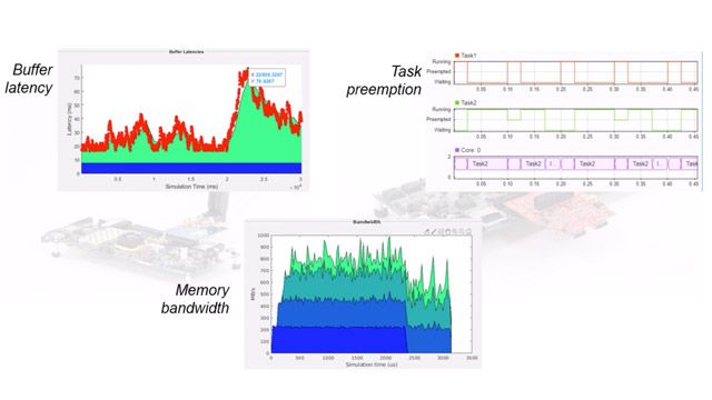
The example used in this video is the design datapath between hardware logic of an FPGA and an embedded processor using DDR memory. Applications are often partitioned between hardware logic and the embedded processor on system-on-chip (SoC) devices to meet throughput, latency, and processing requirements.
Learn to design and simulate an entire application comprising FPGA and processor algorithms along with memory interfaces. You will see how to use blocks from SoC Blockset to model shared external memory, and how to use SoC Blockset to measure different forms of latency and data loss from memory buffers.
By performing these analyses using simulation, you have better visibility into your design than when just working with hardware. You can uncover issues like loss of throughput, latency, and dropping of samples before implementing on hardware.
Modeling and Simulation Use SoC Blockset to design and simulate applications with FPGA and processor algorithms and memory interfaces before deploying to hardware.

Xilinx Deployment Use SoC Blockset to deploy a complete hardware/software application to a Xilinx ZC706 development board.
You can also select a web site from the following list
Americas
- América Latina (Español)
- Canada (English)
- United States (English)
Europe
- Belgium (English)
- Denmark (English)
- Deutschland (Deutsch)
- España (Español)
- Finland (English)
- France (Français)
- Ireland (English)
- Italia (Italiano)
- Luxembourg (English)
- Netherlands (English)
- Norway (English)
- Österreich (Deutsch)
- Portugal (English)
- Sweden (English)
- Switzerland
- United Kingdom (English)
Asia Pacific
- Australia (English)
- India (English)
- New Zealand (English)
- 中国
- 日本Japanese (日本語)
- 한국Korean (한국어)