Single Ended Via Analysis with Placement of Ground Return Vias for 40+ Gbps Signaling
This example shows how to model the return path of single ended printed circuit board vias using the viaSingleEnded object.
The viaSingleEnded object combines a detailed, efficient model of the via return path to enable analysis of the effect of nearby ground return vias (GRVs) on the high frequency performance of the signal via. As demonstrated through measurement and modeling [1, 2], GRVs can produce resonances at high frequencies. This example shows how to reproduce the results that was modeled in [1]. You can also use the viaSingleEnded object to model crosstalk in differential vias [3].
For more information, see Eigenmode-Based Solver for PCB Vias.
Board set-up
The structure being examined is a single PCB layer for a "square" single-ended via site, as shown in the figure below. Black circles represent the via sites, showing how the single-ended traces route to these vias. Grey circles indicate the Ground Return Vias (GRVs) [1].

A single ended via is surrounded by a 2mm square of GRVs. There are additional GRVs outside of the square, and this example shows you how to model a total of eight GRVs in this pattern.
This example gradually builds the structure under study by adding one or more GRVs in each section, starting with one GRV. Each section shows the analysis and results for the geometry in that section so that you can observe how the via response changes with each additional GRV or GRVs.
Next section shows you how to describe the board geometry and materials programmatically.
Board Parameters
Define board dimensions
d = 1.9990e-04; % Via barrel diameter, m
D = 7.8892e-04; % Antipad diameter, m
vSignalViaAntipad = shape.Circle('Radius',D/2);
vSignalViaPad = shape.Circle('Radius',2.5e-4);
kbi0_ch0 = [0 0]; % Signal Via Locations, m
kbi0_ch0_grv = [-1e-3 1e-3;-1e-3 -1e-3;1e-3 -1e-3;1e-3 1e-3]; % Ground Return Via Locations, m
Material properties of Megtron 7
Define a dielectric object that describes the propagation constant as a function of frequency for the dielectric used in the layer containing the via [4].
Er = 3.15; % Dielectric permittivity
tand = 2e-3; % Dielectric loss tangent
T = 2.2027e-04; % Dielectric layer thickness, m
fspec = 1e9; % Dielectric frequency specification, Hz
sub = dielectric(Name="MEG7",EpsilonR=Er,LossTangent=tand,Thickness=T,...
    Frequency=fspec,FrequencyModel="DjordjevicSarkar") % Substrate
sub =
  dielectric with properties:

              Name: 'MEG7'
          EpsilonR: 3.1500
       LossTangent: 0.0020
         Thickness: 2.2027e-04
         Frequency: 1.0000e+09
    FrequencyModel: 'DjordjevicSarkar'

For more materials see catalog
Computation of S-parameters of the Via Structures
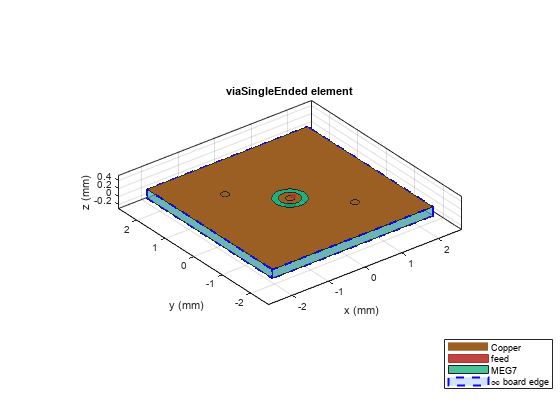
One single ended via with one GRV
This section builds the via with a single GRV, computes the S parameters for that site and displays the S parameters and the site geometry.
The viaSingleEnded object is constructed using a series of name/value pairs to set the object Properties. The Substrate Property was defined as a dielectric object in the previous section.
vSVLocations = [kbi0_ch0 1 3];
vGRVLocations = [kbi0_ch0_grv(1,:) 1 3];
vPorts = {1 1 d "Vertical";...
    1 3 d "Vertical"};
Create a viaSingleEnded:
obj = viaSingleEnded(...
    "SignalLayer",[1 3],...
    "GroundLayer",[1 3],...
    "Substrate",sub,...
    "SignalViaLocations",vSVLocations,...
    "SignalViaDiameter",d,...
    "SignalViaFinishedDiameter",0.9*d,...
    "SignalViaPad",vSignalViaPad,...
    "SignalViaAntipad",vSignalViaAntipad,...
    "GroundReturnViaLocations",vGRVLocations,...
    "GroundReturnViaDiameter",d,...
    "GroundReturnViaFinishedDiameter",0.9*d,...
    "SignalTable",vPorts)
obj =
  viaSingleEnded with properties:

   Conducting Layers
                        SignalLayer: [1 3]
                        GroundLayer: [1 3]
                          Conductor: [1×1 metal]

   Dielectric Layers
                          Substrate: [1×1 dielectric]

   Signal Vias
                 SignalViaLocations: [0 0 1 3]
                  SignalViaDiameter: 1.9990e-04
          SignalViaFinishedDiameter: 1.7991e-04
                       SignalViaPad: [1×1 shape.Circle]
                   RemoveUnusedPads: 1
                   SignalViaAntipad: [1×1 shape.Circle]

   Ground Return Vias
           GroundReturnViaLocations: [-1.0000e-03 1.0000e-03 1 3]
            GroundReturnViaDiameter: 1.9990e-04
    GroundReturnViaFinishedDiameter: 1.7991e-04

   Ports
                        SignalTable: {2×4 cell}
Display PCB structure
Use the show function to display geometry of the object.
figure
show(obj)

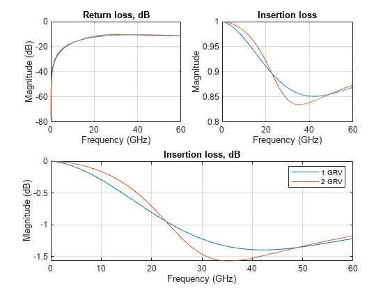
Plot Return Loss and Insertion Loss with 1 GRV
Use the S-parameter function to calcluate return and insertion loss of the viaSingleEnded object containing 1 signal via and 1 GRV.
df = 10e6;
fmax = 60e9;
nfreq = ceil(fmax/df);
f = linspace(df,fmax,nfreq);
Z0 = 50;
S_1grv = sparameters(obj,f,Z0,'Behavioral',true);
% Return loss in dB
figure(1)
ax1 = subplot(2,2,1);
rfplot(ax1,S_1grv,1,1,"db")
title(ax1,'Return loss, dB')
legend(ax1,"hide")
hold(ax1,"on")

% Insertion loss
ax2 = subplot(2,2,2);
rfplot(ax2,S_1grv,1,2,"abs")
title(ax2,'Insertion loss')
legend(ax2,"hide")
hold(ax2,"on")

% Insertion loss in dB
ax3 = subplot(2,2,[3 4]);
ln = rfplot(ax3, S_1grv,1,2,"db");
ln.DisplayName = sprintf('%d GRV',size(obj.GroundReturnViaLocations,1));
title(ax3,'Insertion loss, dB')
hold(ax3,"on")

Two GRVs
This section adds a second GRV diagonal from the first GRV.
vGRVLocations = [kbi0_ch0_grv([1 3],:) repmat([1 3],2,1)];
obj.GroundReturnViaLocations = vGRVLocations;
Display PCB structure
figure
show(obj)
Plot Return Loss and Insertion Loss with 2 GRVs
Observe that the insertion loss is reduced at lower frequencies but increased at higher frequencies.
S_2grv = sparameters(obj,f,Z0,'Behavioral',true);
rfplot(ax1,S_2grv,1,1,"db")
legend(ax1,"hide")
rfplot(ax2,S_2grv,1,2,"abs")
legend(ax2,"hide")
ln = rfplot(ax3,S_2grv,1,2,"db");
ln.DisplayName = sprintf('%d GRV',size(obj.GroundReturnViaLocations,1));
Three GRVs
This section adds another GRV, making a total of three GRVs.
vGRVLocations = [kbi0_ch0_grv([1 2 3],:) repmat([1 3],3,1)];
obj.GroundReturnViaLocations = vGRVLocations;
Display PCB structure
figure
show(obj)

Plot Return Loss and Insertion Loss with 3 GRVs
Note that while the insertion loss is further reduced at low frequencies, a distinct notch has formed around 37GHz.
S_3grv = sparameters(obj,f,Z0,'Behavioral',true);
rfplot(ax1,S_3grv,1,1,"db")
legend(ax1,"hide")
rfplot(ax2,S_3grv,1,2,"abs")
legend(ax2,"hide")
ln = rfplot(ax3,S_3grv,1,2,"db");
ln.DisplayName = sprintf('%d GRV',size(obj.GroundReturnViaLocations,1));

Four GRVs
vGRVLocations = [kbi0_ch0_grv repmat([1 3],4,1)];
obj.GroundReturnViaLocations = vGRVLocations;
Display PCB structure
figure
show(obj)

Plot Return Loss and Insertion Loss with 4 GRVs
S_4grv = sparameters(obj,f,Z0,'Behavioral',true);
rfplot(ax1,S_4grv,1,1,"db")
legend(ax1,"hide")
rfplot(ax2,S_4grv,1,2,"abs")
legend(ax2,"hide")
ln = rfplot(ax3,S_4grv,1,2,"db");
ln.DisplayName = sprintf('%d GRV',size(obj.GroundReturnViaLocations,1));

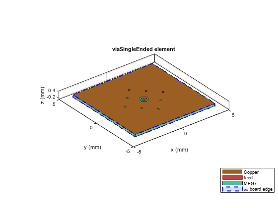
Eight GRVs
The code in this section defines an additional four GRV locations and adds them to the four GRV locations of the previous section.
reftable = zeros(8,2);
kbi0_0_grvmm_p1 = [-2e-3 0;2e-3 0;0 2e-3;0 -2e-3];
reftable(1:4,1:2) = kbi0_ch0_grv;
reftable(5:8,1:2) = kbi0_0_grvmm_p1;
vGRVLocations = [reftable repmat([1 3],8,1)];
obj.GroundReturnViaLocations = vGRVLocations;
Display PCB structure
figure
show(obj)
Plot Return Loss and Insertion Loss with 8 GRVs
The notch depth at 37 GHz has gotten even deeper. The notch depth has now reached 8 dB.
S_8grv = sparameters(obj,f,Z0,'Behavioral',true);
rfplot(ax1,S_8grv,1,1,"db")
legend(ax1,"hide")
rfplot(ax2,S_8grv,1,2,"abs")
legend(ax2,"hide")
ln = rfplot(ax3, S_8grv,1,2,"db");
ln.DisplayName = sprintf('%d GRV',size(obj.GroundReturnViaLocations,1));
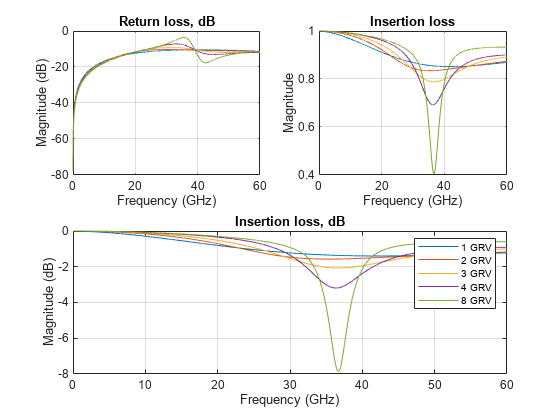
From the insertion loss plot, we can see that the onset frequency of the resonant behavior increases as the number of GRVs increases. The rapid IL decrease near the ¼ wavelength frequency of the GRVs is seen even in this small structure.
Transmission Path Discontinuities
Plot the time-domain response (TDR) for the "square" GRV pattern (i.e., signal via with 4 GRVs). The mathematical model is not bandwidth-limited, so TDR is computed at 40 GHz and also extended to 60 GHz. The TDR results show that signals with higher data and/or spectral content can expect to experience a significantly higher discontinuity. This is due to the inductive behavior of the via under study.
f40 = 40e9;
tdr40 = tdr(S_4grv,RiseTime=1/f40,SampleTime=1/(100*f40),EndTime=0.1e-9);
plot(tdr40)
ylim([48 68])
text(0.08,58,'40 GHz')
f60 = 60e9;
tdr60 = tdr(S_4grv,RiseTime=1/f60,SampleTime=1/(100*f60),EndTime=0.1e-9);
plot(tdr60)
ylim([48 68])
text(0.08,60,'60 GHz')
Discussions
The progression from one GRV to eight GRVs demonstrates the formation of a resonant cavity around the via. At low frequencies, the GRVs combine in parallel to reduce the total impedance of the via return path. However, at higher frequencies, they form resonatant cavity which acts as an open circuit.
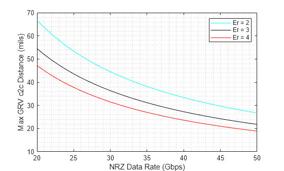
Designers of printed circuit boards for high frequency signals should be aware of this phenomenon and determine whether it will occur for the frequencies and distances they are considering. One conservative metric is the Gap Rate Distance (GRD) metric [1], defined as the maximum center-to-center distance between a signal via and its closest associated GRVs for a given data rate, based on guard bands. As long as at least some GRVs are closer than the GRD, the design should be safe.
The following code computes and plots the GRD for different dielectric constants. According to the plot of this metric, for a dielectric constant of 3.0 and a maximum frequency of 35GHz, the design will be safe (by a conservative margin) if there is at least one GRV closer than 0.030” (0.75mm).
Er = [2 3 4]; % Sweep across relative Permittivity
freq = linspace(1.0e10,2.5e10,101); % Sweep across frequencies
cw = 0.16; % Critical wavelength set at 0.16 accounting in guard band
clr = ["c" "k" "r"]; % Color of line handles
for i = 1:numel(Er)
    obj.Substrate.EpsilonR = Er(i);
    grd = obj.gapratedistance(2*freq,cw);
    plot(2*freq/1e9,grd,clr(i),'DisplayName',join(["Er =",num2str(Er(i))]))
    hold on
end
grid('minor')
xlabel('NRZ Data Rate (Gbps)')
ylabel('Max GRV c2c Distance (mils)')
legend('show')
References
Steinberger, Michael, Telian, Donald, Tsuk, Michael, Iyer, Vishwanath, and Yanamadala, Janakinadh. "Proper Ground Return Via Placement for 40+ Gbps Signaling". Signal Integrity Journal (December 27, 2024). https://www.signalintegrityjournal.com/articles/2858-proper-ground-return-via-placement-for-40-gbps-signaling
Tucker, Sankararaman, and Ellis, “PCB Stackup and Launch Optimization in High-Speed Designs”, DesignCon 2022, April 2022.
Steinberger, Telian, Bloom and Rowett, “Managing Differential Via Crosstalk and Ground Via Placement for 40+ Gbps Signaling”, DesignCon 2023, February 2023.
Djordjevic, Biljic, Likar-Smiljanicand, and Sarkar, “Wideband Frequency-Domain Characterization of FR-4 and Time-Domain Causality”, IEEE Transactions on Electromagnetic Compatibility, Vol. 43, No. 4, pg. 662-7, November 2001.