Model Design for AXI4 Register Interface Generation
To perform lightweight data transfer or to access control registers, use AXI4 register interfaces. The AXI4 register interfaces include the AXI4 and AXI4-Lite interfaces. With the HDL Coder™ software, you do not have to implement AXI4 or AXI4-Lite protocol in your model. The software generates AXI4 or AXI4-Lite interfaces in the HDL IP core.
When you model your design, specify the data ports, you want to map to the AXI4 register interfaces. HDL Coder then maps the data ports to memory-mapped registers and allocates address offsets for the ports.
Considerations
When you map your DUT ports to AXI4 or AXI4-Lite interfaces:
You can map all scalar, vector, or bus ports in your design to either AXI4 or AXI4-Lite interfaces.
You cannot map some DUT ports to AXI4 interfaces and other DUT ports to AXI4-Lite interfaces for the same design.
Map Scalar Ports to AXI4 Register Interface
When you use scalar data types at the DUT interface ports, you can directly map the interface ports to AXI4 or AXI4-Lite interfaces. The code generator assigns a unique address to each data port that you want to map to the AXI4 interface.
For an example that shows how to map scalar ports to AXI4-Lite interfaces, open the
model
hdlcoder_led_blinking.
openExample('hdlcoder/IPCoreGenWorkflowWithAMicroBlazeProcessorKC705Example',...
'supportingFile','hdlcoder_led_vector.slx')

In this model, the subsystem led_counter is the hardware subsystem.
It models a counter that blinks the LEDs on an FPGA board. Two input ports,
Blink_frequency and Blink_direction, are
control ports that determine the LED blink frequency and direction. All the blocks
outside of the subsystem led_counter are for software
implementation.
In Simulink®, you can use the Slider Gain block or the Manual
Switch block to adjust the hardware subsystem's input values. The
ARM® processor controls the generated IP core by writing to the AXI interface
accessible registers in the embedded software. The output port of the hardware subsystem
connects to the LED hardware. You can use the output port Read_back
to read data back to the processor.
When you run the IP Core Generation workflow, in the Set
Target Interface task, you see that the ports
Blink_frequency, Blink_direction, and
Read_back map to AXI4-Lite interfaces.
To learn more about this example, see:
Map Vector Ports to AXI4 Subordinate Interface
When you use vector data types at the DUT interface ports, you can directly map the interface ports to AXI4 or AXI4-Lite interfaces. The code generator assigns a unique address for each data port that you want to map to the AXI4 interface.
When you map vector ports, HDL Coder uses additional strobe registers for each port to maintain the synchronization with the IP core algorithm logic. For input ports, the strobe registers control the enable signals for a set of shadow registers, making the IP core algorithm logic see the updated vector elements simultaneously. For output ports, the strobe registers make sure that the vector data to be read is captured synchronously.
For an example that shows how to map vector ports to AXI4-Lite interfaces, open the
model
hdlcoder_led_vector.
open_system('hdlcoder_led_vector')
In this model, the subsystem DUT implements the LED blinking
algorithm and has vector output ports. When you run the IP Core
Generation workflow, you see that the input ports and output ports map to
AXI4-Lite interfaces in the Set Target Interface task.
To learn more, see IP Core Generation Workflow with a MicroBlaze Processor.
Map Double Data Types and Data Larger than 32 bits to AXI4 Register Interfaces
When your DUT port has double data types or data types with width greater than 32 bits, HDL Coder:
Splits the data into individual 32 bit words to match the register width of the AXI4 or AXI4-Lite interface.
Assigns each 32 bit word to an individual address. You can find the resulting start and end addresses in the IP Core Generation report under the Register Address Mapping section.
Creates an additional strobe register to synchronize the data at the DUT boundary. The strobe logic behaves the same as the strobe register for vector ports. For more information on how vector ports are handled, see Map Vector Ports to AXI4 Subordinate Interface.
Learn how HDL Coder splits and maps data with bit widths greater than 32 bits to individual addresses. In this example model there are three input ports and three output ports:
Input and output port one: Scalar with
uint64datatype.Input and output port two: Scalar with
ufix45_En10datatype.Input and output port three: Vector of three elements with 64 bit datatype.
This image shows the example DUT with the corresponding datatypes on the input and output ports. Each port is mapped to the AXI4 interface.

When HDL Coder processes the DUT it converts the data into 32 bit words and maps each 32 bit word to a specific address. This image shows the target interface configuration and register address mapping sections of the generated IP core report. The register address mapping section mentions the start address, number of 32 bit words and the final register address for data with bit widths greater than 32 bits.
For input port one the 64 bit data is split into two 32 bit words. The two words are
mapped to addresses 0x100 and 0x104. Bits zero
through 31 are mapped to 0x100 and bits 32 through 63 are mapped to
0x104. Output port one is split across addresses
0x148 and 0x14C.
For input port two the 45 bit data is split into two 32 bit words. The two words are
mapped to addresses 0x110 and 0x114. Bits zero
through 31 are mapped to 0x110 and bits 32 through 63 are mapped to
0x114. Output port two is split across addresses
0x158 and 0x15C.
For input port three, each vector element is split into two 32 bit words. This results in a total of six 32 bit words for the entire vector. The six words are mapped to the addresses 0x120, 0x124, 0x128, 0x12C, 0x130, and 0x134.
Bits zero through 31 of the first vector element are mapped to 0x120.
Bits 32 through 63 of the first vector element are mapped to 0x124.
Bits zero through 31 of the second vector element are mapped to 0x128.
Bits 32 through 63 of the second vector element are mapped to 0x12C.
Bits zero through 31 of the third vector element are mapped to 0x130.
Bits 32 through 63 of the third vector element are mapped to 0x134.
Output port three is split into 6 32 bit words. The six words are mapped to addresses 0x180, 0x184, 0x188, 0x18C, 0x190, 0x194.
Map Complex Data Types to AXI4 Register Interface
When your DUT port has complex data types, HDL Coder:
Extracts the real and imaginary parts of the complex data and converts them into two separate elements.
Assigns these elements to two consecutive memory addresses. The lower address stores the real part, and the subsequent address stores the imaginary part of the complex data being transmitted. The Register Address Mapping section of the IP core generation report specifies the start and end addresses.
Creates an additional strobe register to synchronize the data at the DUT boundary. The strobe logic behaves the same as the strobe register for vector ports. For more information about vector ports, see Map Vector Ports to AXI4 Subordinate Interface.
For complex vector data or data types wider than 32 bits, it uses a single strobe to synchronize all of the data elements.
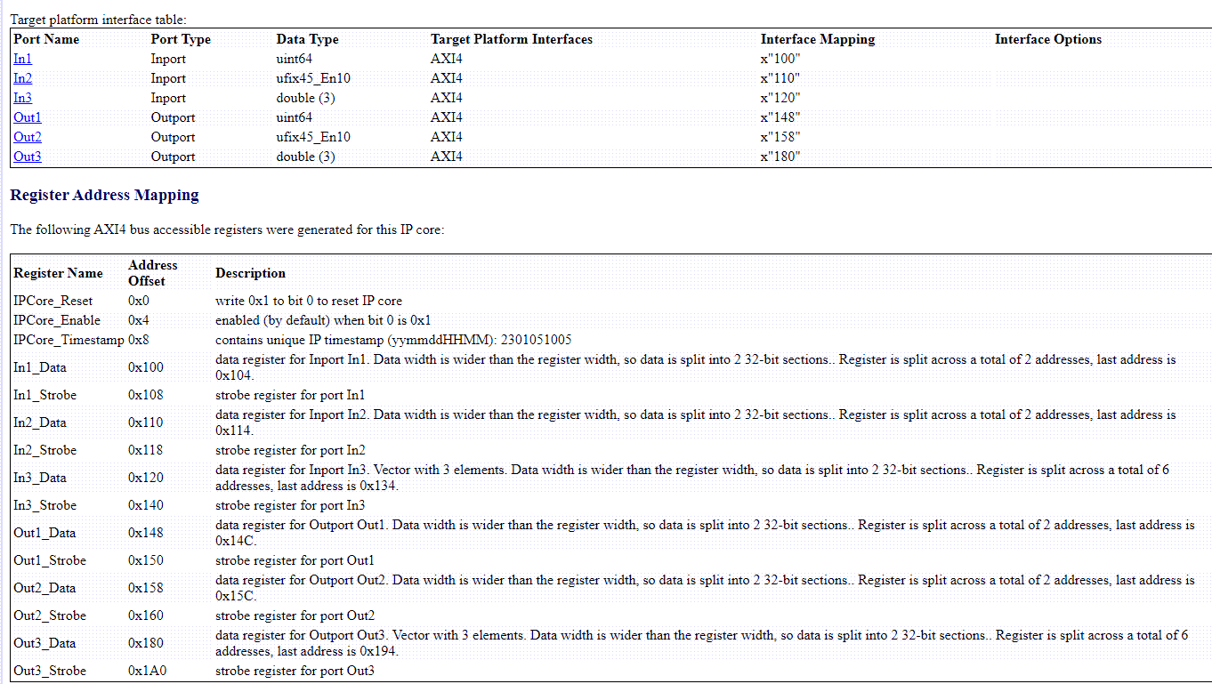
For example, for a DUT port that has complex scalar data with a bit-width less than
32, HDL Coder extracts the real and imaginary parts of each data port and converts them
into a two-element vector. HDL Coder then assigns each element an address. This image
illustrates this process for a complex scalar with int16 data type.
HDL Coder splits the 16-bit complex signal into two 32-bit words and maps the two words
to addresses 0x128 and 0x12C. The software then maps bits zero through 15 of the real
part to 0x128 and bits 0 through 15 of the imaginary part to 0x12C. The strobe register
controls the enable signals for a set of shadow registers, allowing the IP core
algorithm logic to see the updated real and imaginary signals simultaneously. For output
ports, the strobe register ensures that the complex data is captured synchronously,
synchronizing the real and imaginary parts.
For a DUT port that has complex scalar data with a bit-width greater than 32,
HDL Coder splits the real and imaginary elements into 32-bit words to fit the
register width of the AXI4 or AXI4-Lite interface. This image illustrates a complex
scalar with uint64 data type. HDL Coder splits the 64-bit complex
signal into four 32-bit words and maps the four words to addresses 0x190, 0x194, 0x198,
and 0x19C. The software then maps bits zero through 31 of the real part to 0x190 and
bits 32 through 63 of the real part to 0x194. It maps bits zero through 31 of the
imaginary part to 0x198 and bits 32 through 63 of the imaginary part to 0x19C. A single
strobe synchronizes all the data elements.

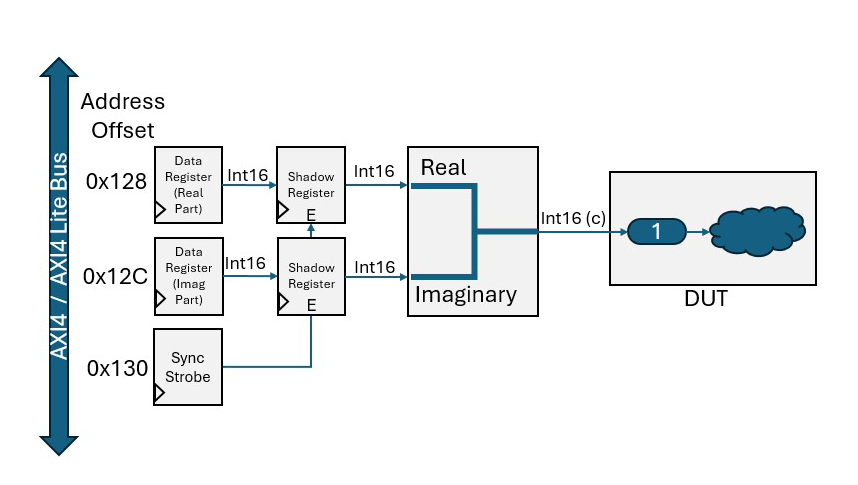
For a DUT port that has complex vectors, HDL Coder splits each vector element into real and imaginary elements, then further
splits each element into 32-bit words to fit the register width of the AXI4 or AXI4-Lite
interface. This image illustrates a complex vector with two elements of
uint32 data type each. The software then maps bits 0 through 31
of the real part of the first vector element to 0x100 and bits 0 through 31 of the real
part of the second vector element to 0x104. It maps bits 0 through 31 of the imaginary
part of the first vector element to 0x108 and bits 0 through 31 of the imaginary part of
the second vector element to 0x10C. The strobe register synchronizes the real and
imaginary parts.
For output ports, the strobe register controls the synchronous capturing of the data to be read.
Map Bus Data Types to AXI4 Register Interface
When you use bus data types at the DUT interface ports, you can directly map the interface ports to AXI4 or AXI4-Lite interfaces.
When you map a port with bus data types to an AXI4 register interface, HDL Coder assigns a unique address for each bus element. HDL Coder treats bus ports as a group of independent scalar and vector ports. When HDL Coder assigns an address to bus elements, they are treated as separate registers and the addresses are not contiguous. When you change the address of a bus port in the target interface table, only the address of the first element changes.
Model Bus Element
Model a bus element by using a bus creator block or bus element block to create a bus port.
Model a bus element by using a bus creator block.

Model a bus element by using bus element blocks: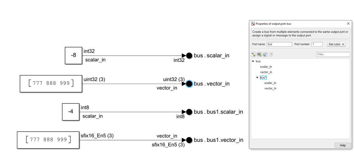
For more information, see Map Bus Data Types to a Register Interface.
Specify Initial Value of AXI4 Registers
When you run the IP Core Generation workflow or the
Simulink Real-Time FPGA I/O workflow, you can specify an initial
value for input ports mapped to the AXI4 registers. You can specify an
initial value when mapping to these target interfaces:
AXI4
AXI4-Lite
PCIe
When you map tunable parameter ports to AXI4 registers, you cannot specify the initial value. By default, the initial value is zero. To specify a nonzero value:
In the target platform interface table, when you map an input DUT port to an AXI4 register interface, an Options button appears in the Interface Options column.
Click the Options button, and then specify the RegisterInitialValue.
The specified value is saved on the DUT Inport blocks as the HDL block property
IOInterfaceOptions in the Target
Specification tab. For example, if you map a DUT input port to AXI4-Lite
interface, set RegisterInitialValue to 5, and
then run the Set Target Interface task. The
IOInterfaceOptions property of that input port is saved with
the value {'RegisterInitialValue','5'}.
To view the IOInterfaceOptions value, if the full path to your
DUT port is hdlcoder_led_blinking/led_counter/LED,
enter:
hdlget_param('hdlcoder_led_blinking/led_counter/LED',...
             'IOInterfaceOptions')
Specify the initial value for scalar ports.
hdlset_param('hdlcoder_led_blinking/led_counter/LED', ...
     'IOInterfaceOptions', {'RegisterInitialValue','5'});
To set the initial value for a bus, specify a struct whose field names match the bus
element names. For example,
You can also specify the initial value by using a variable defined in the MATLAB® workspace. For example:
bus1_initialvalue = struct('scalar_in1',1,'scalar_in2',2,'scalar_in3',3,'scalar_in4',4,'vector_in',[1 3])
Read Back Value of AXI4 Register Interfaces
When you run the IP Core Generation workflow, you can read back the
value that is written to the AXI4 registers by using the AXI4 register
interface. For example, you can read back the values that are written to the AXI4
subordinate registers by using the devmem command in the Linux® console of the ARM processor. If you have HDL Verifier™ installed, you can use the AXI Manager IP to read back the values.
To use this capability, in the Generate RTL Code and IP Core task of the IP Core Generation workflow, select the Enable readback on write registers check box, and then run the Generate RTL Code and IP Core task
When you run this task, HDL Coder saves the read back setting that you enabled on the model. In the HDL
Block Properties of the DUT Subsystem, on the IP Core Parameter
section of the Target Specification tab, you see a parameter
WriteRegisterReadback set to on. If you
export the HDL Workflow Advisor run to a script, you see this setting saved on the model
by using
hdlset_param.
hdlset_param('hdlcoder_led_vector/DUT', 'WriteRegisterReadback', 'on');
These examples show how you can read back values by using the
devmem command in the Linux console with a program such as PuTTy™.
To read back values when mapping scalar ports to AXI4 interfaces, you first write values to the AXI4 registers, and then read back the values. You can see the memory address of the AXI4 registers in the IP Core Generation report.

To read back values when mapping vector ports to AXI4 interfaces, you first write to
the AXI4 registers, then write the strobe register address with 0x1,
and then read back the values. You can see the memory address of the AXI4 registers and
the strobe register in the IP Core Generation report.

Optimize Timing on Register Interface
Since R2024b
When your model contains several output registers and you want to read back data from multiple AXI4 registers, the read-back logic can impact the synthesis frequency. After you build the bitstream, if the timing closure is not met and the critical path is in the read address decoder, or you want to convert the decoder architecture from a single multiplexer to multiple ones prior to running synthesis, you can optimize the timing by adjusting the Register interface read pipeline parameter.
When you set Register interface read pipeline to a non-zero value, HDL Coder generates a balanced multiplexer tree with the specified pipeline registers and converts the decoder architecture from a single multiplexer to multiple multiplexers. The default value is zero, which translates into a single multiplexer. When you set the parameter to a non-zero value, HDL Coder determines the number of levels in the multiplexer tree based on the maximum read register address, and divides the address space evenly. If the resulting number of levels is less than the specified pipeline value, the optimization places additional pipeline registers at the end of the multiplexer tree to match the number of pipeline registers specified by the Register interface read pipeline parameter. You can set the Register interface read pipeline parameter in:
Task 3.2. Generate RTL Code and IP Core of the HDL Coder Workflow advisor.
The Interface Settings tab of the IP Core Editor.
The MATLAB command line by using the
hdlset_paramto set theRegisterInterfaceReadPipelineparameter.The HDL Block Properties of the DUT
For example, this image illustrates how, if you have a DUT with ten read ports and you set Register interface read pipeline to zero, HDL Coder generates a single level multiplexer with zero pipelines.
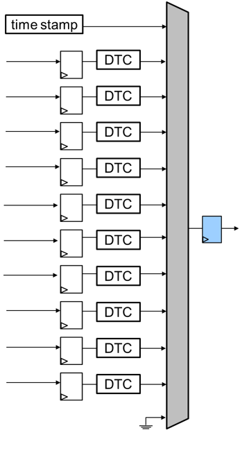
When you set Register interface read pipeline to three, HDL Coder creates a four level multiplexer tree and inserts pipelines between each level of multiplexers.

The default read delay for the AXI4 register interface is one clock cycle. When you
specify a different value for Register interface read pipeline, the
read delay for each AXI4 register interface is n
clock cycles, where n is the number of register interface read
pipelines plus one. The IP core report contains the timing diagram and
information.

If you generate an IP core for a model created before R2024b, and
AXI4 Slave port to pipeline register
ratio is a non-zero value, HDL Coder sets Register interface read pipeline to
0.
Limitations
The AXI4 register interfaces do not support simultaneous read and write transactions.
You cannot map some DUT ports to AXI4-Lite interfaces while mapping others to AXI4 interfaces within the same design.
The write strobe signal of the AXI4 protocol must be fully asserted (all high) for the AXI4 register interface to accept the transaction. When an AXI4 master initiates a write transaction to the AXI4 register interface in the generated IP core without the write strobe fully asserted, the AXI4 register interface discards the transaction.