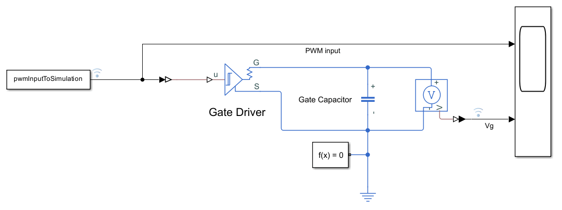
Gate Driver
Behavioral model of gate driver integrated circuit

Libraries:
Simscape /
Electrical /
Semiconductors & Converters
Description
The Gate Driver block provides an abstracted representation of a gate driver integrated circuit. The block models input hysteresis, propagation delay, and turn-on/turn-off dynamics. Unless modeling a gate driver circuit explicitly, always use this block or the Half-Bridge Driver block to set gate-source voltage on a MOSFET block or gate-emitter voltage on an IGBT block. Do not connect a controlled voltage source directly to a semiconductor gate, because this omits the gate driver output impedance that determines switching dynamics.
You can model electrical or physical signal input ports by setting the Modeling option parameter to either:
PS input— The driver output state is controlled by a physical signal input u. Use this modeling option if all of your controller, including PWM waveform generation, is determined by Simulink® blocks. This modeling option is the default.Electrical input ports— The driver output state is controlled by two electrical input connections, PWM and REF. Use this option if your model has upstream analog components, such as the Controlled PWM Voltage source.
When the input rises above the logic 1 input level, the transition of the output state from off to on is initiated after a delay equal to the turn-on propagation delay. The demanded output voltage across the G and S ports steps in value from the off-state output voltage to the on-state output voltage, but the actual output voltage is set by the RC time constant associated with the On-state gate drive resistance value and the total load capacitance. Similarly, when the input falls below the logic 0 input value, the transition of the output state from on to off is initiated after a delay equal to the turn-off propagation delay and with dynamics now set by the Off-state gate drive resistance value.
Faults
To model a fault in the Gate Driver block, in the Faults section, click Add fault next to the fault that you want to model. For more information about fault modeling, see Fault Behavior Modeling and Fault Triggering.
You can insert a fault into the output of the gate driver at a specified simulation time, to make the connected semiconductor device either permanently off or permanently on. Use this feature to represent a failed semiconductor device as failed at open-circuit or at normal on-state conditions.
Examples

HEV PMSM Drive Test Harness
A test harness for a Permanent Magnet Synchronous Motor (PMSM) drive sized for use in a typical hybrid vehicle. The test harness can be used to determine overall drive losses when operating at a given speed and torque. Tabulated losses information from this test harness can then be used by the Simscape™ Electrical™ Motor & Drive (System Level) block for rapid simulation of complete drive cycles whilst still accurately predicting overall system efficiency.
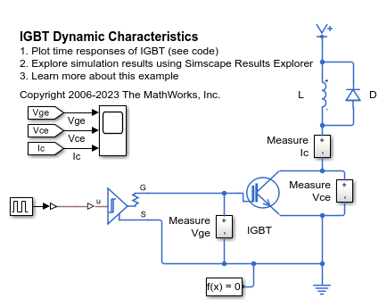
IGBT Dynamic Characteristics
How the dynamic characteristics of an IGBT depend on its parameters. A prerequisite to matching dynamic characteristics to datasheet values or measured data is to set the parameters defining the static I-V curve. For this, see the 'IGBT Characteristics' example, IGBTCharacteristics. With static parameters correctly set, the dynamic parameters can then be set as follows:
Parameterize Gate Driver from SPICE Netlist
Parameterize the Simscape Electrical Gate Driver block from a manufacturer netlist using LTspice.

Three-Phase High-Power Converter Design and Analysis Workflow
The main steps involved in designing a high-power converter. High power converters are important building blocks for future electric mobility and microgrid solutions. To design a cost effective, lightweight, efficient converter, you must perform detailed analysis of different converter design options and deployment scenarios. This example helps you to simulate the steady state, transient electrical, and thermal characteristics of a three-phase two-level converter that uses Insulated-Gate Bipolar Transistor (IGBT) devices.
Ports
Input
Conserving
Parameters
Extended Capabilities
Version History
Introduced in R2017b