WLAN Receiver Using AMD RFSoC Device
This example shows how to simulate and deploy a WLAN HDL receiver system and retrieve the signal and data field information from a WLAN signal in Simulink® using an SoC Blockset™ implementation targeted on a AMD® Zynq® UltraScale+™ RFSoC ZCU111 evaluation board.
Using this example, you can integrate HDL Implementation of WLAN Receiver (Wireless HDL Toolbox) example into the SoC Blockset implementation.
Supported Hardware Platforms
AMD Zynq UltraScale+ RFSoC ZCU111 evaluation kit + XM500 Balun card
Design Task
In this example, the design task is to build a WLAN receiver and implement the system on an AMD RFSoC device. This example shows the workflow for designing, simulating, and deploying the WLAN receive algorithm on the hardware. This figure shows the conceptual overview of the example.
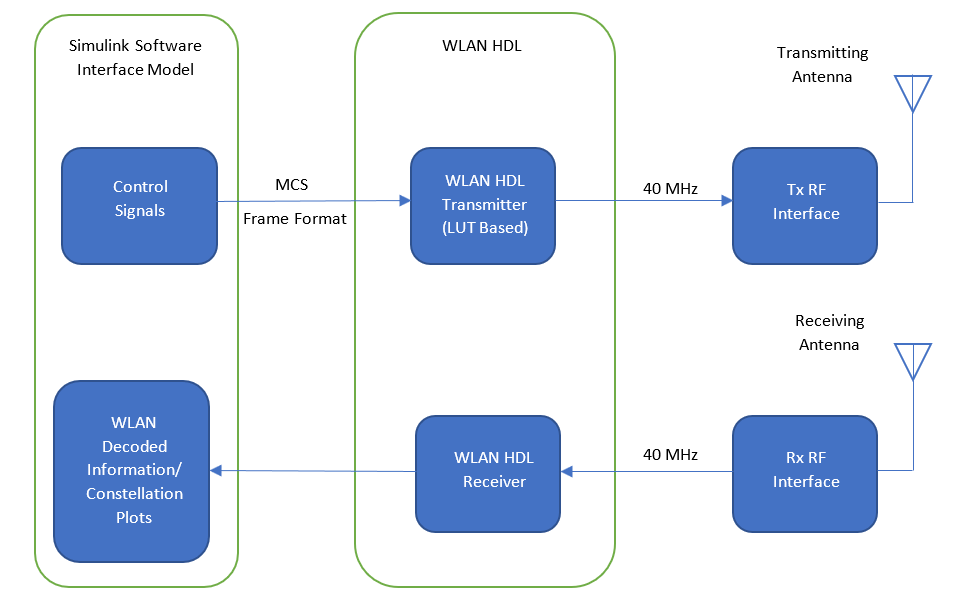
The WLAN HDL Transmitter and the WLAN HDL Receiver blocks perform high-speed signal processing tasks and make the WLAN algorithm well- suited for FPGA implementation on the programmable logic (PL) of the radio platform. To implement this algorithm on the PL, the example uses the Simulink® hardware model from the HDL Implementation of WLAN Receiver (Wireless HDL Toolbox) example with binary convolutional coding (BCC).
Design Using SoC Blockset
Create an SoC model soc_WLAN_top as the top model and set the Hardware board to Xilinx Zynq UltraScale+ RFSoC ZCU111 evaluation kit. The top model includes FPGA model soc_WLAN_fpga and processor model soc_WLAN_proc, which are instantiated as model references. The top model also includes AXI4-Stream to Software block that shares the external memory between the FPGA and the processor.
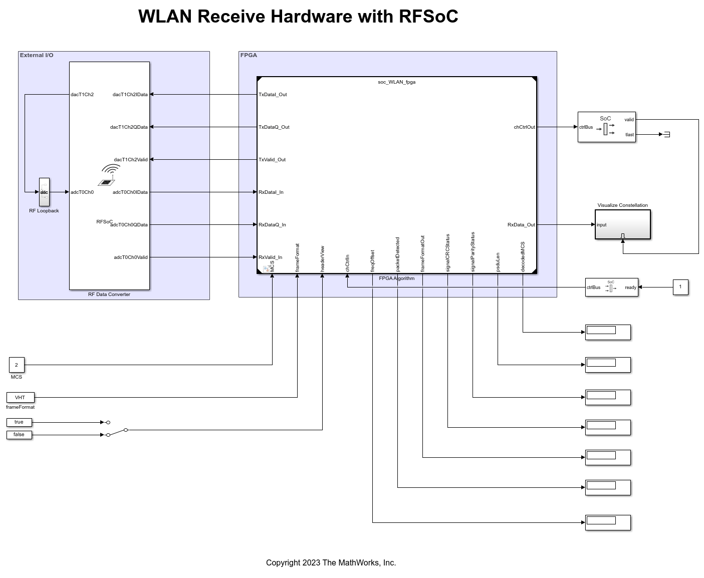
Create an SoC model soc_WLAN_hwtop as the top model to simulate the hardware algorithm with a static configuration. This model includes an FPGA model soc_WLAN_fpga.
RF Data Converter Configuration
An RFSoC device has its RF data converter connected to the PL. To configure the analog to digital converter (ADC) and digital to analog converter (DAC) settings, use the RF Data Converter block. The block provides an interface to the AMD RF Data Converter IP in Simulink to model a wireless system destined for implementation on a AMD RFSoC device.
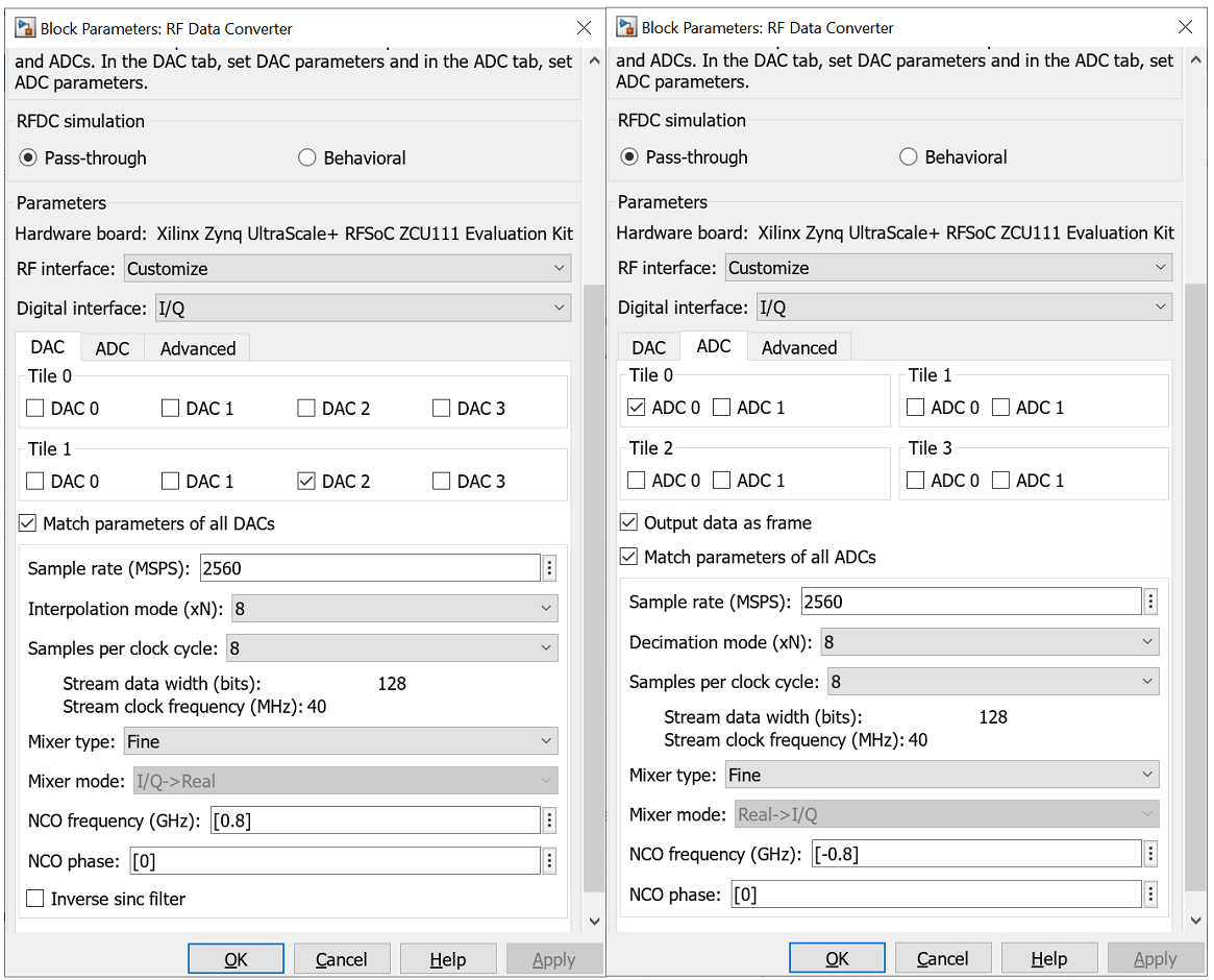
To meet the 800 MHz RF carrier frequency and 40 MSPS baseband sample rate, configure the RF Data Converter block according to the settings described here and shown in the figure. Set the NCO frequency parameter for the DAC and ADC mixers to 0.8 GHz, and set the DAC and ADC sample rate to 2560 MSPS. Choose the values of Interpolation mode (xN), Decimation mode (xN), and Samples per clock cycle parameters such that the effective clock cycle (sample rate) for the wireless algorithm FPGA is the desirable value. For this example, the desired value is 40 MSPS. This value is calculated and displayed on the block mask as the Stream clock frequency (MHz) parameter after you click Apply. Set the Decimation mode (xN) parameter to 8. The effective sample rate after decimation is 320 MSPS. To get the clock cycle (baseband sample rate) to 40 MSPS, set the Samples per clock cycle parameter to 8. Similarly, in the DAC tab, set the Interpolation mode (xN) parameter to 8 and the Samples per clock cycle parameter to 8. With these settings, the Stream clock frequency parameter is 2560/(8*8) = 40 MHz.
Hardware Logic Design
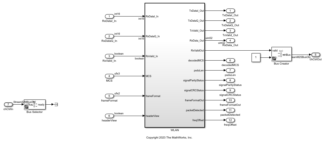
The FPGA model soc_WLAN_fpga contains three subsystems: Vector Interpolation (which is connected to the DAC portion of the RFDC block), Vector Decimator (which is connected to the ADC portion of the RFDC block), and WLAN HDL.

The Vector Decimator block receives the packed eight samples as 128 bits. The Vector Decimator block decimates input vector samples by 8 and sends them to the WLAN HDL subsystem. The sample rate after the Vector Decimator block is 40 MSPS, as expected by WLAN HDL subsystem for its processing.
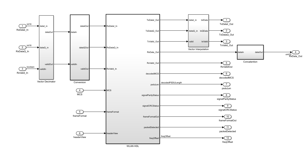
The WLAN HDL subsystem has two sections: WLAN Transmit and Receive section and Status Signal Generator section. The WLAN Transmit and Receive section includes WLAN_Tx_Rx, Prepare Inputs, and Prepare Outputs subsystems.
The WLAN_Tx_Rx subsystem includes WLAN_Tx, Decimator, and WLAN_Rx subsystems.
The
WLAN_Txsubsystem is a variant subsystem and it containsWLAN_Tx_20MHzandWLAN_Tx_40MHzsubsystems that are implemented using lookup tables (LUTs). Based on the channel bandwidth value, the model selects eitherWLAN_Tx_20MHzorWLAN_Tx_40MHzsubsystem. TheWLAN_Tx_20MHzsubsystem contains LUT data corresponding to modulation and coding schemes (MCS) from 0 to 7 for non-high-throughput (non-HT), high-throughput (HT), and very-high-throughput (VHT) frame formats. TheWLAN_Tx_40MHzsubsystem contains LUT data corresponding to MCS 0 to 7 for HT and VHT frame formats.
The
Decimatorsubsystem decimates the input data by 2 for 20 MHz channel bandwidth option and for 40 MHz channel bandwidth option this subsystem sends the input data as it is.
The
WLAN_Rxsubsystem is implemented from the HDL Implementation of WLAN Receiver (Wireless HDL Toolbox) example with BCC support.
In the receive path, the Vector Decimator block receives the packed eight samples with a sample rate of 320 MSPS from the RF Data Converter block. The Vector Decimator block decimates input vector samples by 8 and sends them to the WLAN receiver. The sample rate after the Vector Decimator block is 40 MSPS, as expected by the WLAN_Tx_Rx subsystem for its processing. The WLAN Receiver block sends the processed data to the processor with a sample time of 40 MHz. In the transmit path, the WLAN Transmitter block sends the samples to the RF Data Converter block through the Vector Interpolation block. The Vector Interpolation block interpolates the input samples by 8 (320 MSPS) and sends them to the RF Data Converter block as a vector of eight samples.
Processor Logic Design
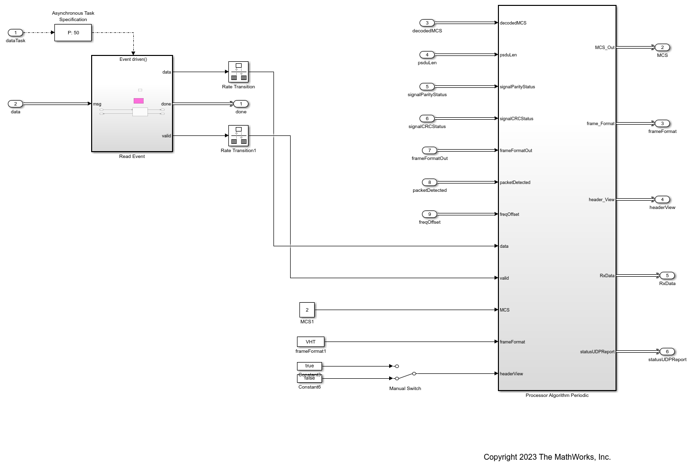
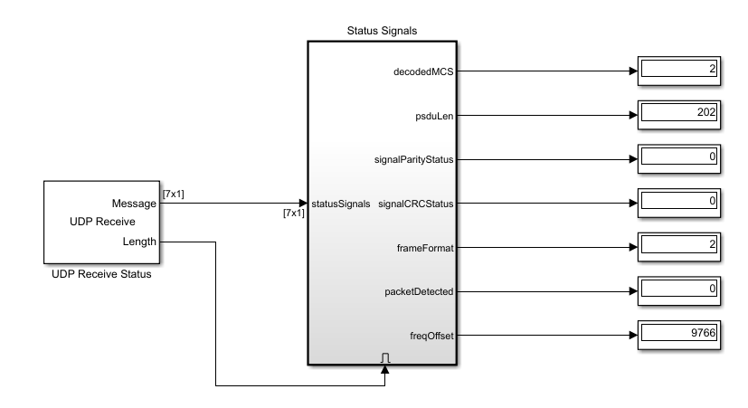
The processor logic contains a read task and a periodic task. The periodic task is a timer-driven task with a periodic time of 1e-2, which is defined in the task manager. The periodic task drives the control and status signals of the hardware algorithm through the AXI4-Lite registers. The model displays status information such as the frame format, MCS, PSDU length, signal parity, signal CRC, packet detected status, and estimated frequency offset (in Hz) from the WLAN receiver. The controller provides the constellation data and status information to the MATLAB host by using UDP blocks. The RxUDPData and StatusUDPData subsystems relay the constellation and status signals, respective to the host over the UDP protocol.
The read task is an event-based task driven by the arrival of data from the FPGA through DDR memory. This data comprises the constellation data of the selected modulation type. The previous two tasks are modeled under the Processor Algorithm Wrapper subsystem in processor model soc_WLAN_proc and are connected to the Task Manager block at the top level.
Host Model
The host model receives the output of the WLAN Receiver block, data and receiver status signals from the processor model over the Ethernet link by using UDP Write blocks. The IP address of the UDP Write block in the processor model must be configured with the IP address of the host. This interface model, which runs on the host, shows how to receive data from the hardware platform and how to postprocess it.

Simulate
To confirm its basic operation, run the hardware generation model.
Because the model contains a large number of HDL-optimized blocks, and these HDL-optimized blocks require simulation using sample-based signals. It takes a while for the simulation. The figure shows the constellation diagram from the simulation.
If you want to see the complete hardware and software simulation of the WLAN receive algorithm and the controller dynamic configuration, run the soc_WLAN_top model. Run the host model to see the receiver status signals and constellation diagram.
Implement and Run on Hardware
Hardware Setup
Connect the SMA connector on the XM500 Balun card to complete the loopback between the DAC and ADC, according to these connections: DAC229_T1_CH2 (J5) to ADC224_T0_CH0 (J4).
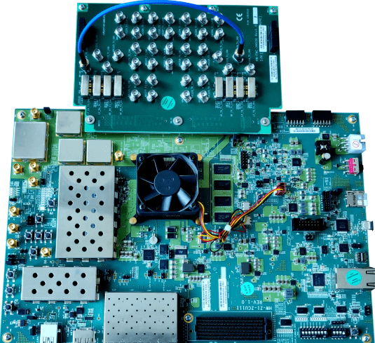
To implement the model on a supported SoC board, use the SoC Builder tool. Ensure that the Hardware Board option is set to Xilinx Zynq UltraScale+ RFSoC ZCU111 Evaluation Kit on the System on Chip tab of the Simulink Toolstrip.
To open SoC Builder, click Configure, Build, & Deploy. After the SoC Builder tool opens, follow these steps.
On the Setup screen, select Build Model and click Next.
On the Review Memory Map screen, click View/Edit Memory Map to view the memory map and then click Next.
On the Select Project Folder screen, specify the project folder and then click Next.
On the Select Build Action screen, select Build External mode and then click Next.
On the Validate Model screen, click Validate to check the compatibility of the model for implementation and then click Next.
On the Build Model screen, click Build to begin building the model. An external shell opens when FPGA synthesis begins. Click Next.
On the Connect Hardware screen, click Test Connection to test the connectivity of the host computer with the SoC board. Click Next to go to the Run Application screen.
FPGA synthesis can take more than 30 minutes to complete. To save time, you can use the provided pregenerated bitstream by following these steps.
Close the external shell to terminate FPGA synthesis.
Copy the pregenerated bitstream to your project folder by entering this command at the MATLAB command prompt.
copyfile(fullfile(matlabshared.supportpkg.getSupportPackageRoot,'toolbox','soc','supportpackages','xilinxsoc','xilinxsocexamples','bitstreams','soc_WLAN_top-XilinxZynqUltraScale_RFSoCZCU111EvaluationKit.bit'),'./soc_prj');
Click Load and Run to load the pregenerated bitstream and run the model on the SoC board. After the bit file is loaded, open the generated software model.
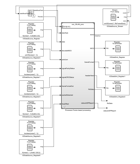
Run the model in external mode by clicking Monitor & Tune. You can control the configuration from the Simulink model.
Constellation and Status Signals from Hardware
Run the host model to see the received constellation data and receiver status signals. When the host interface model runs successfully, the model displays the constellation diagram and status signals.

Run MATLAB Interface Script
You can control the deployed design using a MATLAB script running on the host. The Prototype Generated IP Core on Hardware using FPGA I/O (HDL Coder) example shows how the HDL Coder™ software generates the interface definition function and the connection between MATLAB and the FPGA. SoC Builder generates the gs_soc_WLAN_top_setup function inside the project folder. This function is copied into the runWLANRxHardware script.
The runWLANRxHardware script implements the MATLAB control of the deployed design using the generated interface. The script writes control signals to the FPGA and reads results from the FPGA, displays plots, and displays results in a table.


Things to Try
By default, the example runs for the 20 MHz WLAN channel bandwidth option. For 40 MHz channel bandwidth option, in Model Properties > InitFcn callback of the soc_WLAN_hwtop model, assign channelBW to '40MHz', and run the model to verify the hardware algorithm with simulation. To generate the bit file and verify the example on hardware, in Model Properties > InitFcn callback of the soc_WLAN_top model, assign channelBW to '40MHz', and then follow the steps in the Implement and Run on Hardware section.
To verify the algorithm at 2.4 GHz RF carrier frequency, in the RF Data Converter block, set the NCO frequency parameter for the DAC and ADC mixers to 2.4 GHz and elect the corresponding high frequency DAC and ADC tiles such as DAC 0 or DAC 1 in Tile 1 and ADC 0 or ADC 1 in Tile 1. To eliminate the image frequencies after RF Data Converter, use a suitable band-pass filter at 2.4 GHz.
Connect the SMA connector on the XM500 Balun card to complete the loopback based on the selected DAC or ADC mixer. If the selected DAC mixer is either DAC 0 or DAC 1 in Tile 1, use DAC229_T1_Ch0 (J7) or DAC229_T1_Ch1 (J8) and if the selected ADC mixer is either ADC 0 or ADC 1 in Tile 1, use ADC225_T1_Ch0 (J2) or ADC225_T1_Ch1 (J1) to complete the loopback connection.
Conclusion
This example shows how to integrate the WLAN receive algorithm on an AMD ZCU111 evaluation board using the SoC Blockset implementation and how to verify the design in simulation and on hardware.