Multi-Channel Transceiver Using Xilinx RFSoC Device
This example shows how to implement a multi-channel transceiver using RF Data Converter on a Xilinx® RFSoC device. The RFSoC devices have multiple channels of DAC and ADC. This enables you to design complex communication systems that require multiple transceivers. In this example, you simulate a model that contains an RF Data Converter block with two DAC and ADC channels that have different configurations. This example uses the WLAN and 5G NR waveforms as test inputs. You can also observe the effects of RF Data Converter configuration on the input waveforms.
Supported Hardware Platforms
Xilinx® Zynq™ UltraScale+™ RFSoC ZCU111 Evaluation Kit + XM500 balun card
Introduction
Using the IP core generation workflow, you can focus on the algorithm component and integrate it in a predefined reference design that defines the architecture. Use this workflow for rapid prototyping when a reference design that meets your system requirements is available for deployment. Following are the reference designs available for the Xilinx Zynq UltraScale+ RFSoC ZCU111 Evaluation Kit, Xilinx Zynq UltraScale+ RFSoC ZCU208 Evaluation Kit, and Xilinx Zynq UltraScale+ RFSoC ZCU216 Evaluation Kit.
Real ADC/DAC Interface
IQ ADC/DAC Interface
Model Structure
On the top level, this example model consists of three subsystems RF Data Converter, Transceiver Algorithm, and Stream To Channels. In Transceiver Algorithm, on the transmit side, Single Port RAM blocks are initialized with pre-generated 5G NR and WLAN waveforms. These waveforms are generated using Wireless Waveform Generator app, 5G NR waveform is generated with 20 MHz bandwidth at a sample rate of 40 MHz, WLAN waveform is generated with 40 MHz bandwidth at a sample rate of 40 MHz. Then the data from the RAM blocks is interpolated by 8 to achieve the required sample rate at DAC. Then the interpolated data is transmitted through two different digital-to-analog converter (DAC) channels of the RFSoC device. Then the DAC channels inside the RF Data Converter block interpolates the input data and shifts their center frequency to the provided NCO frequency. Then the data is loop back to analog-to-digital converter (ADC) channels in the RF Data Converter block. Then the output from ADC channels is send back to the Transceiver Algorithm subsystem. In Transceiver Algorithm, on the receive side, the received data is decimated by 8 to get the actual rate with which we transmitted the waveforms. Then the Stream To SW subsystem concatenates the data received from the two channels and stream to the processing system.
This example is configured with "IQ ADC/DAC Interface" reference design to run on Xilinx Zynq UltraScale+ RFSoC ZCU111 Evaluation Kit.
RF Data Converter Configuration for channel 1:
Uses DAC Tile 0 Channel 1 and ADC Tile 2 Channel 1
Sample rate = 1280 MSPS
Interpolation/decimation mode = 4
Samples per clock cycle = 8
Mixer frequency = 0.5 GHz
RF Data Converter Configuration for channel 2:
Uses DAC Tile 1 Channel 0 and ADC Tile 1 Channel 0
Sample rate = 2560 MSPS
Interpolation/decimation mode = 8
Samples per clock cycle = 8
Mixer frequency = 2.1 GHz
open_system('soc_multiChannelTransceiver')
![]()
close_system('soc_multiChannelTransceiver')
Simulation
Simulate the model and observe the spectrum in all spectrum analyzer blocks.
Channel 1 (WLAN waveform)
Transmitted signal

RF signal

Received signal

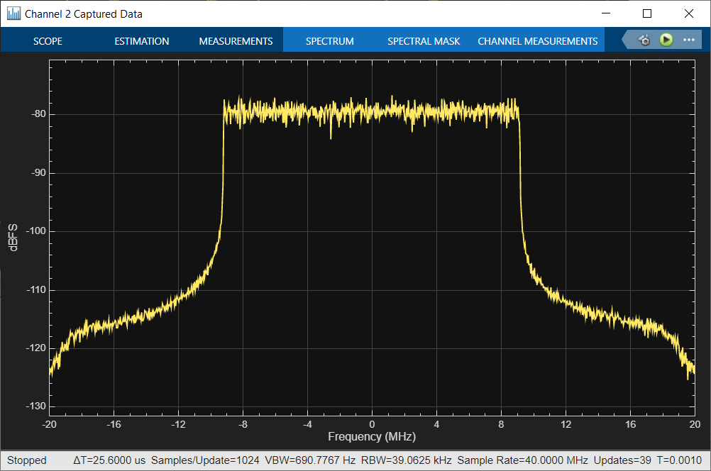
Channel 2 (5G NR waveform)
Transmitted signal

RF signal

Received signal
Implementation
Hardware Setup for ZCU111 Kit
Connect the SMA connectors on the XM500 balun card to complete the loop back between the DACs and ADCs, according to the connections provided in the following table. Use DC blocks for differential channels loop back.

To implement the model on a supported SoC board, use the HDL Coder™ IP core generation workflow. To add the HDL Code tab to the Simulink toolstrip, open the Apps gallery and select HDL Coder.
In the Configuration Parameters dialog box of the model, set the HDL workflow, target platform, and reference design by following these steps.
1. In the left pane, expand HDL Code Generation and then select Target.
2. Set Workflow to IP Core Generation.
3. Set Target Platform to Xilinx Zynq UltraScale+ RFSoC ZCU111 Evaluation Kit. Ensure that the Synthesis Tool is set to Xilinx Vivado.
4. Ensure that the Reference Design parameter is set to IQ ADC/DAC Interface.
5. Ensure that the AXI4-Stream Master data width parameter under Reference Design Settings is set to 64.
6. As the model has an RF Data Converter block, all the parameter values provided in the RF Data Converter block are considered for code generation. If model has no such block, then the reference design parameters are considered for code generation.

To automatically map the interface of the IP, follow these steps.
1. Identify the IP core subsystem for code generation by selecting the Transceiver Algorithm subsystem.
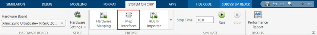
2. On the System On Chip tab, click Map Interfaces.
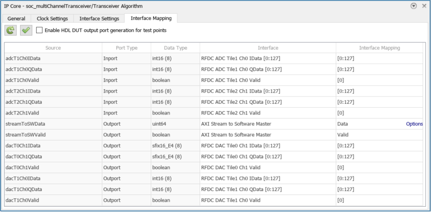
To view and edit the generated IP core interface mapping, follow these steps.
1. On the HDL Code toolstrip tab, click Target Interface.
2. In the IP Core panel, on the Interface Mapping tab, click the refresh button to load the mapping.
3. Edit the mapping until you map each DUT port and the mapping table appears as shown below.
4. Click the check button to validate the mapping.

Generate the HDL IP core and the FPGA bitstream files by following these steps.
1. On the HDL Code tab, click Build Bitstream.
2. After the HDL IP core generation finishes, an external shell opens for FPGA synthesis. Wait for the synthesis to complete. The FPGA synthesis often takes more than 30 minutes to complete.
For more information about the IP core generation workflow, see Get Started with IP Core Generation from Simulink Model (HDL Coder).
Run on Hardware
Program the FPGA on the SoC board by following these steps.
1. To download the bitstream, in the Simulink Toolstrip, on the HDL Code tab, select Build Bitstream > Program Target Device.
2. Verify your generated IP core on the hardware by using the generated host interface script. This script contains MATLAB commands that connect your hardware and interact with your IP core. To generate a host interface script file, in the Simulink Toolstrip, in the HDL Code tab, select Host Interface Script > Host Interface Script.
3. After downloading the bitstream, run the soc_multiChannelTransceiver_hw_interface.m script (modified version of the generated host interface script) to get the data back to the host from the hardware.
Summary
This example shows how to implement a multi-channel transceiver on a Xilinx RFSoC device. You simulate the model and go though the workflow required to implement it on a Xilinx RFSoC platform.