Introduction To Custom OFDM Using AMD RFSoC
This example shows how to deploy a custom OFDM transmitter and receiver algorithm to an AMD® ZCU111 RFSoC development board, using SoC Blockset™. The example builds on the Introduction to Custom OFDM (Wireless HDL Toolbox) example, adding the infrastructure and connectivity around the transmitter and receiver to implement the design on hardware. MATLAB® is used to control, analyze and verify the behavior of the design.
Simulink Model
The soc_IntroOFDM.slx model implements the custom OFDM design for targeting an RFSoC. The model includes the device under test (DUT) subsystem for code generation, and a testbench to validate the design in simulation. The model requires the constants defined by the setup_soc_introOFDM.m script. The PostLoadFcn model callback runs the script when you load the model. The top level of the model is shown.

The DUT subsystem integrates the OFDM Transceiver, Radio and Utilities, and Data Interface subsystems.
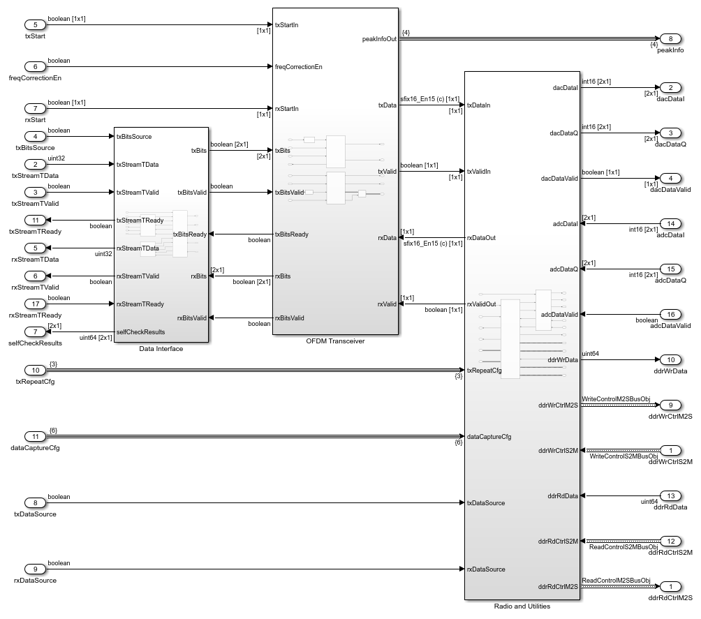
OFDM Transceiver
The OFDM Transceiver subsystem contains the OFDM Transmitter, OFDM Receiver, and the Transmit Control subsystems.
The
OFDM TransmitterandOFDM Receiversubsystems implement the core OFDM algorithm. TheTransmit Controlsubsystem controls the pacing of the transmitter to generate the required sample rate. The design runs at a clock rate ofradioClockRate=245.76 MHz, and the transmitter sample rate isofdmSampleRate=7.68 MHz. Therefore, theTransmit Controlsubsystem enables the transmitter for one clock cycle out of245.76/7.68=32clock cycles.For more information on the transmitter and receiver implementations see the Introduction to Custom OFDM (Wireless HDL Toolbox) example.

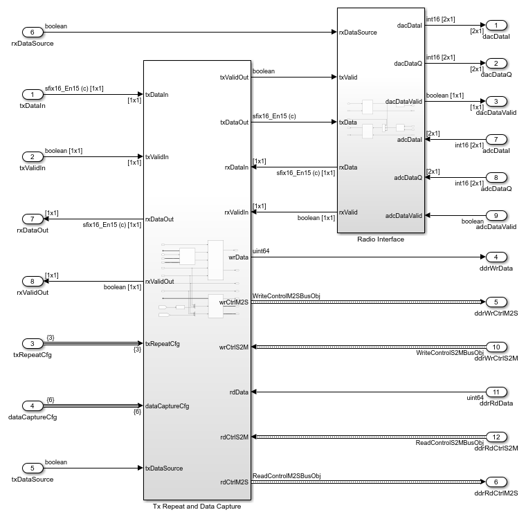
Radio and Utilities
The Radio and Utilities subsystem contains the Radio Interface, and Tx Repeat and Data Capture subsystems.
The
Radio Interfacesubsystem connects the transmit and receive waveform data to the RF data converter. TheRadio Interfacesubsystem containsDDCandDUCsubsystems to convert between theofdmSampleRateof the transceiver and theradioSampleRateof the radio. The digital downconverter (DDC) and digital upconverter (DUC) use the architecture from the Implement Digital Downconverter for FPGA (DSP HDL Toolbox) and Implement Digital Upconverter for FPGA (DSP HDL Toolbox) examples. The filter coefficients are optimized for the sample rates used in this example. TherxDataSourceport selects the input source for the DDC. Set the port to0to use theRF Data Converteroutput, or set the port to1to use theDUCoutput.The
Tx Repeat and Data Capture/Transmit Repeatsubsystem implements transmit repeat by reading a pre-generated waveform from external memory. The waveform can be written to external memory from MATLAB as a setup step during verification. ThetxDataSourceport selects the input source for the DUC. Set the port to0to use theOFDM Transmitteroutput, or set the port to1to use theTransmit Repeatoutput.The
Tx Repeat and Data Capture/Data Capturesubsystem implements data capture by writing the capture data to external memory. Data can be captured from the transmit data at the output of theOFDM Transmitter, the received data at the input of theOFDM Receiver, and the equalized data symbols from theOFDM Receiver. One of these signals can be captured at a time. The captured data can be read back to MATLAB for analysis during verification.
Data Interface
The Data Interface subsystem implements the interfaces used to provide input bits to the transmitter, and read output bits from the receiver. The AXI-Stream subsystem connects the transmit and receive bits to the embedded processor. The AXI-Stream subsystem inserts a fixed 64-bit header, 0x493B075609CE6F6C, to the transmit bits at the start of each OFDM frame's payload, and checks the header in the received bits. The header pattern reduces the probability of false positives with a noisy signal. The received bits are only sent to the output stream if the header matches the expected constant. Additionally, the Data Interface subsystem contains a Self-Check subsystem. The Self-Check subsystem verifies the design by generating a known bit sequence for the transmitter and comparing the received bits to the expected sequence. The Self-Check subsystem outputs the number of received bits, and bit errors. This is used to calculate the bit error rate (BER) of the received data. Set the txBitsSource port to 0 or 1 to use the AXI-Stream or Self-Check data source, respectively.
Generate and Deploy Hardware Configuration Files
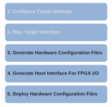
To generate and deploy the hardware configuration files for the AMD ZCU111 RFSoC, use the HDL Coder™ IP core generation workflow. The workflow steps are shown. The model is pre-configured with the required target settings and interface mapping for steps 1 and 2 respectively. For more information on configuring a model to target an RFSoC with the IP core workflow see the Transmit and Receive Tone Using IP Core Generation Workflow on RFSoC Device example.
Generate Hardware Configuration Files
To add the HDL Code Simulink toolstrip tab, open the Apps tab and click HDL Coder.
On the HDL Code tab, click Build Bitstream.
After HDL IP core generation finishes, an external shell opens for FPGA synthesis, implementation and bitstream generation.
The workflow outputs the design artifacts in the
soc_prjfolder.
The table shows the resource utilization results after implementation. The design meets timing with a clock frequency of 245.76 MHz.
       Resource        Usage
    _______________    _____

    Slice Registers    92840
    Slice LUTs         60599
    RAMB18                19
    RAMB36                69
    DSP48                102
Generate Host Interface For FPGA I/O
To verify the generated bitstream on the hardware use MATLAB to generate the host interface for FPGA I/O. For more information on using FPGA I/O see the Use FPGA I/O to Rapidly Prototype HDL IP Core (HDL Coder) example.
To generate the host interface, in the Simulink Toolstrip, in the HDL Code tab, select Host Interface Script. Two MATLAB files are generated in your current folder.
gs_soc_introOFDM_interface.mis a template for using FPGA I/O to control the deployed design. TherunIntroOFDMHardware.mlive script is a modified version of this template.gs_soc_introOFDM_setup.mconfigures thefpgahardware object with the same ports and interfaces that were pre-configured in the Target Interface table during step 2. The function is used in therunIntroOFDMHardware.mlive script.
Deploy Hardware Configuration Files
To download the hardware configuration files, in the Simulink Toolstrip, in the HDL Code tab, select Build Bitstream > Program Target Device. After programming, the board reboots to apply the changes. After the reboot is complete the deployed design is ready to use.
Verify on hardware
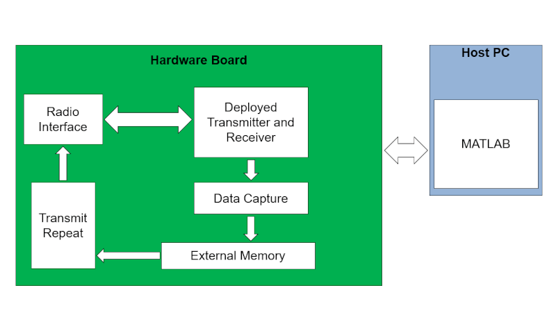
Use the runIntroOFDMHardware.m live script to verify the design on hardware. Before using the runIntroOFDMHardware.m live script you must program the target device with the generated hardware configuration files from the previous section. The example uses FPGA I/O to control the deployed design running live on the target. The example hardware verification setup is shown.
Connect to the FPGA by clicking the "Run hardware connection". This defines the interfaces exposed by FPGA I/O. Once the connection is established, the transceiver on hardware can be used.
Run the transceiver on hardware by clicking the "Run hardware verification" button.
With the default verification setup the transmitter and receiver run in real-time on the hardware target. MATLAB configures control registers for the transmitter and receiver.
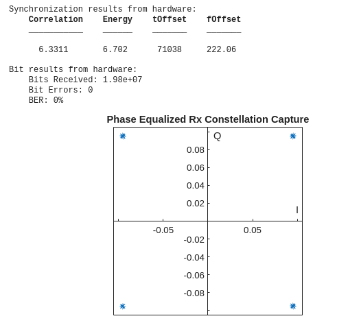
![]()
On a successful run, synchronization results, bit error results, and the equalized data symbol constellation are displayed.
Further Exploration
The runIntroOFDMHardware.m live script contains three additional verification setups. These setups implement steps of a workflow to design and verify SoC implementations of wireless algorithms by enabling rapid and early verification on the target platform.
Transmit Repeat and Post Process In MATLAB - Use this setup to verify the MATLAB algorithms in the presence of real-world impairments.
Deploy Transmitter and Post Process In MATLAB - Use this setup to verify the transmitter implementation.
Transmit Repeat and Deploy Receiver - Use this setup to verify the receiver implementation.
Transmit Repeat and Post Process In MATLAB
To verify the MATLAB algorithms, set the transmitterMode to Transmit Repeat and the receiverMode to Capture to MATLAB. With this setup the generated waveform is transmitted on repeat, and the received waveform is captured and read back into MATLAB. The transmit waveform is generated in MATLAB with introOFDMTx, and the captured receive waveform is post-processed by introOFDMRx. On a successful run, the spectrogram of the captured waveform, synchronization results, timing correlation plot, bit error results, and the equalized data symbol constellation are displayed.
![]()
Deploy Transmitter and Post Process In MATLAB
To verify the transmitter implementation, set the transmitterMode to Deployed and the receiverMode to Capture to MATLAB. With this setup the transmitter runs in real-time on the hardware, and the received waveform is captured and read back into MATLAB. MATLAB configures control registers for the transmitter, and the captured receive waveform is post-processed by introOFDMRx. On a successful run, the spectrogram of the captured waveform, synchronization results, timing correlation plot, bit error results, and the equalized data symbol constellation are displayed.
![]()
Transmit Repeat and Deploy Receiver
To verify the receiver implementation, set the transmitterMode to Transmit Repeat and the receiverMode to Deployed. With this setup the generated waveform is transmitted on repeat, and the receiver runs in real-time on the hardware. The transmit waveform is generated in MATLAB with introOFDMTx, and MATLAB configures control registers for the receiver. On a successful run, synchronization results, bit error results, and the equalized data symbol constellation are displayed.
![]()
The runIntroOFDMHardware.m live script contains additional options to further configure the behavior of the deployed design.
freqCorrectionEn: specifies if frequency correction is performed by the OFDM receiver. Disable or enable the option to set thefreqCorrectionEnport to0or1, respectively.rxDataSource: specifies the data source for the receiver. Set toInternal loopbackto connect the receiver input directly to the output from the transmitter. Set toADCto connect the receiver to the ADC data. To useADCconnect the SMA connectors J7 and J2 on the XM500 balun card to complete the loopback between DAC 0 from tile 1, and ADC 0 from tile 1. Select theADCorInternal Loopbackoption to set therxDataSourceport to0or1, respectively.
File Structure
This example uses these files.
Simulink Models
soc_introOFDM.slx: Implements the algorithm deployed to the FPGA and a testbench to verify the behavior in simulation.
MATLAB live scripts
runIntroOFDMHardware.m: Runs the deployed OFDM transceiver to verify the behavior on the hardware target.
MATLAB code
setup_soc_introOFDM.m: Defines the constants required by thesoc_introOFDM.slxmodel.hardwareIntroOFDM.m: Implements the FPGA I/O control and analysis for each of the verification setups.introOFDMTx.m: Implements the transmitter algorithm in MATLAB. This is used to generate the waveform for transmit repeat.introOFDMRx.m: Implements the receiver algorithm in MATLAB. This is used to post-process the captured received waveform.plotConstellation.m: Creates a constellation plot of complex symbolsmapResetPort.m: Adds the reset port definition to the FPGA I/O interface.packWaveformForDDR.m: Packs a complex waveform to be written to external memory.writeWaveformToDDR.m: Writes a packed waveform to external memory with FPGA I/O.
See Also
AXI4 Random Access Memory | RF Data Converter
Topics
- Create Custom OFDM Resource Grid (Wireless HDL Toolbox)
- Introduction to Custom OFDM (Wireless HDL Toolbox)