Derive RF Data Converter Configuration Using Frequency Planner App
This example shows how to use the Frequency Planner app to derive an RF data converter (RFDC) configuration based on signal specifications required by your design. Because an RFDC has several interdependent parameters that you can configure, deriving its configuration before modeling helps minimize changes to the transmitter and receiver algorithms. In this example, you observe how the RFDC configuration impacts a signal, analyze the signal spectra, optimize configurations to avoid unwanted images or distortion, and export the final settings for use in your design workflow.
Introduction
In wireless communication systems, designing the transmit and receive chains with direct RF sampling data converters is a challenge. In RF transceivers, the transmit path consists of interpolation filters, a complex mixer, and a digital-to-analog converter (DAC). The receive path consists of an analog-to-digital converter (ADC), a complex mixer, and decimation filters. In RFSoC devices, the interpolation and decimation filters, complex mixers, ADC, and DAC are integrated inside the chip as part of the RFDC. This block diagram shows the typical transmit and receive paths.
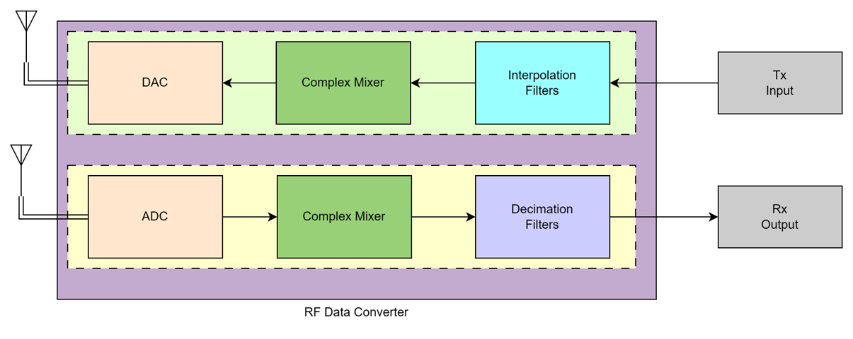
Interpolation filters upsample the input signal by an integer-valued factor. Decimation filters downsample the input signal by an integer-valued factor. A complex mixer shifts the input signal frequency spectrum to center it around the provided carrier frequency (Fc).
The Frequency Planner app guides you through practical scenarios to select appropriate sample rates, interpolation or decimation modes, and NCO frequencies based on your signal requirements.
Open Frequency Planner App
MATLAB Toolstrip: On the Apps tab, under Signal Processing and Audio, click the Frequency Planner app icon.
MATLAB Command Prompt: Enter
frequencyPlanner.Simulink Toolstrip: On the Apps tab, under Signal Processing and Wireless Communications, click the Frequency Planner app icon.
Simulink Toolstrip: On the System on Chip tab, under Prepare, click the Frequency Planner app icon.
Transmitter
Case 1
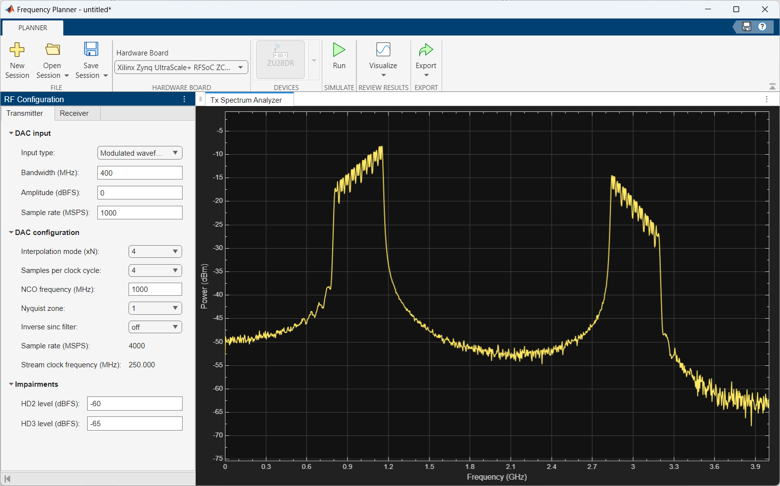
Transmit a baseband signal with a bandwidth of 400 MHz, generated at a sample rate of 1000 MSPS, using a carrier signal of 1000 MHz. Select an interpolation mode of 4x. The final DAC sample rate is 4000 MSPS.
Signal specifications:
Baseband sample rate: 1000 MSPS
Bandwidth: 400 MHz
RFDC configuration:
Interpolation mode: 4x
NCO frequency: 1000 MHz
DAC sample rate: 4000 MSPS
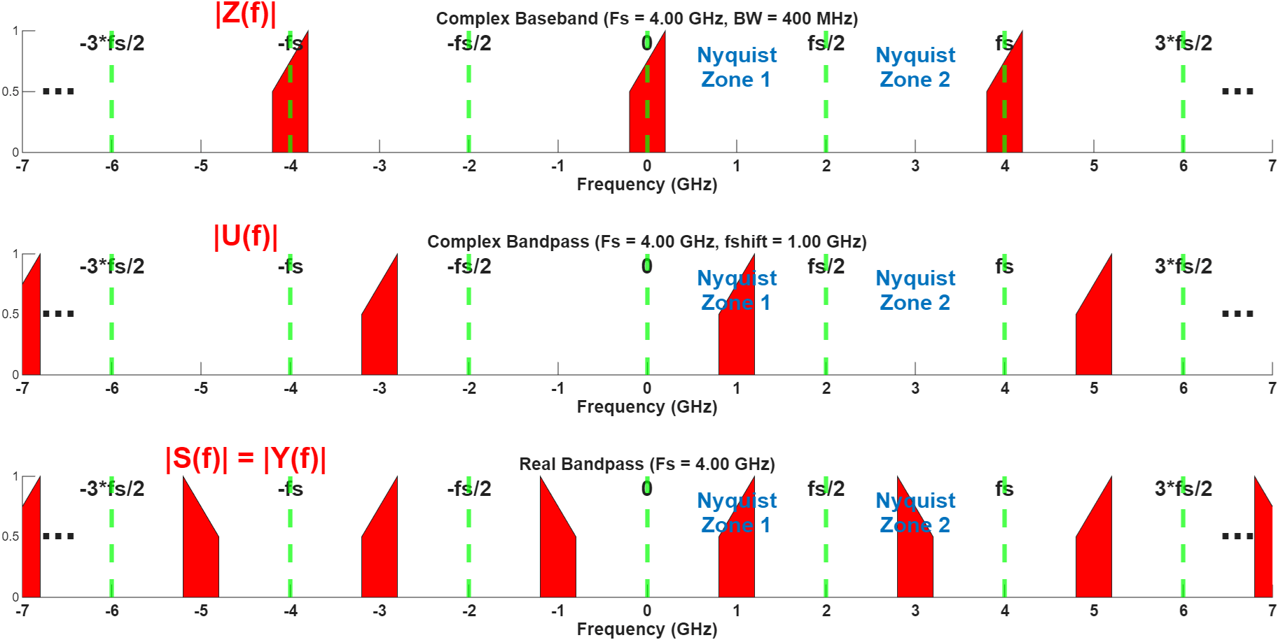
The following figure shows the spectral plot of the signal based on these specifications. The first plot shows the original signal after interpolation, which repeats at every sampling interval. The second plot shows the signal after the mixer stage. As the NCO frequency is 1000 MHz (or 1 GHz), original signal and its images shift to the right by 1000 MHz. The third plot shows the output of the DAC. As the DAC output is real, negative frequencies fold over to the positive side. The signal of interest appears in Nyquist zone 1, and the inverse image appears in zone 2.
Analysis in Frequency Planner
Launch the app and on the Transmitter tab, set Input type to Modulated waveform. Enter the signal specifications and RFDC configuration in the DAC input and DAC configuration panes, respectively. After you select the parameters, click Run to simulate the DAC path. In the Tx Spectrum Analyzer pane, you see the original signal at 1 GHz in Nyquist zone 1, and the inverse image at 3 GHz in Nyquist zone 2. Since a sufficient gap exists between the signal of interest and the image, you can use an analog lowpass filter to remove the image.
Case 2
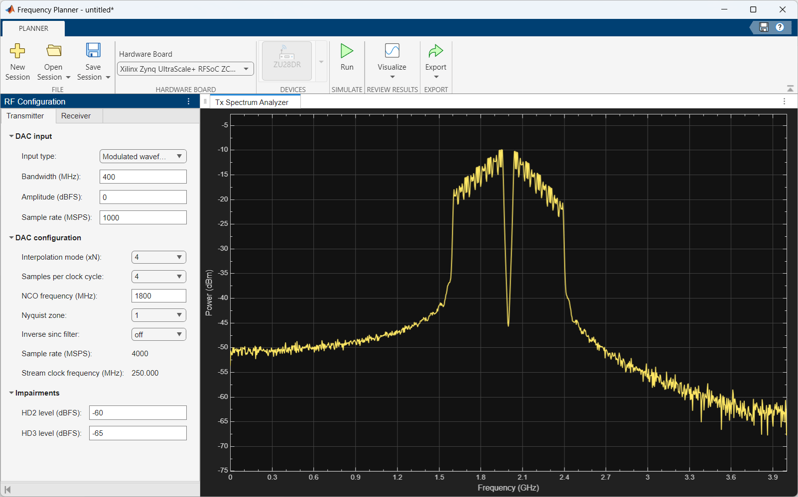
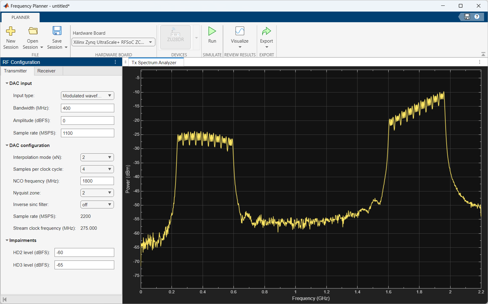
Transmit a baseband signal with a bandwidth of 400 MHz, generated at a sample rate of 1000 MSPS, using a carrier signal of 1800 MHz. Select an interpolation mode of 4x. The final DAC sample rate is 4000 MSPS.
Signal specifications:
Baseband sample rate: 1000 MSPS
Bandwidth: 400 MHz
RFDC configuration:
Interpolation mode: 4x
NCO frequency: 1800 MHz
DAC sample rate: 4000 MSPS
Enter the signal specifications and RFDC configuration in the DAC input and DAC configuration panes in the app. After you select the parameters, click Run to simulate the DAC path. In the Tx Spectrum Analyzer pane, you see the original signal at 1.8 GHz in Nyquist zone 1, and the inverse image at 2.2 GHz in Nyquist zone 2. Since not enough gap exists between the signal of interest and the image, you cannot remove the image using an analog filter.
Solution
To improve the gap between the signal of interest and the image, use the mix-mode capability of the DAC in the RFDC. To do this, reduce the DAC sample rate to 2200 MSPS and change the interpolation mode to 2x. As a result, the baseband sample rate becomes 1100 MSPS, and in the DAC output, the signal of interest appears in Nyquist zone 2. In normal mode, the sinc response of the DAC attenuates the signal in Nyquist zone 2. Mix-mode increases the output power in Nyquist zone 2 while attenuating it in Nyquist zone 1. To enable mix-mode in the DAC, set Nyquist zone to 2.
Signal specifications:
Baseband sample rate: 1100 MSPS
Bandwidth: 400 MHz
RFDC configuration:
Interpolation mode: 2x
NCO frequency: 1800 MHz
DAC sample rate: 2200 MSPS
Nyquist zone: 2
Enter the signal specifications and RFDC configuration in the DAC input and DAC configuration panes in the app. After you select the parameters, click Run to simulate the DAC path. In the Tx Spectrum Analyzer pane, you see the original signal at 1.8 GHz in Nyquist zone 2, and the (attenuated) inverse image at 0.4 GHz in Nyquist zone 1. Since enough gap now exists between the signal of interest and the image, you can remove the image using an analog bandpass filter.
Receiver
Case 1
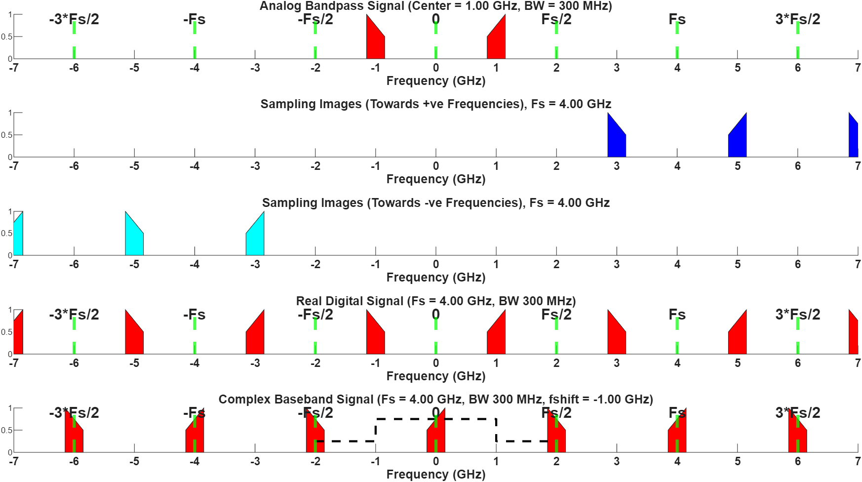
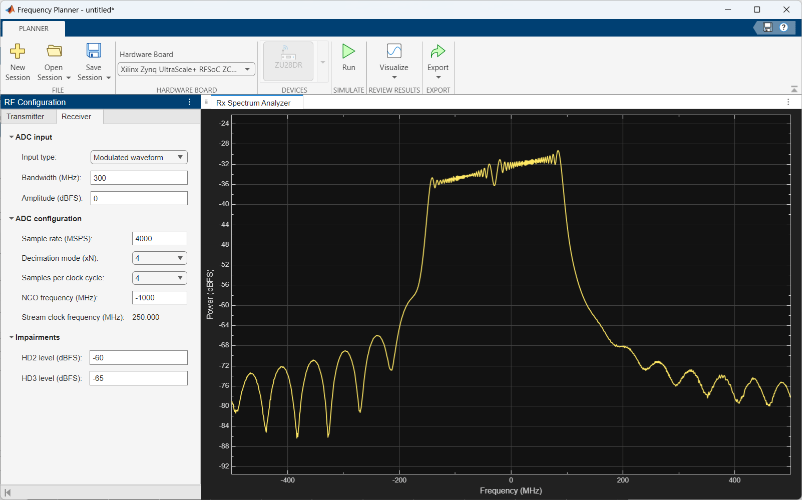
Receive a signal with a bandwidth of 300 MHz, centered at 1000 MHz. Select an ADC sample rate of 4000 MSPS and a decimation mode of 4x. Set the NCO frequency to –1000 MHz.
Signal specifications:
Bandwidth: 300 MHz
RFDC configuration:
ADC sample rate: 4000 MSPS
Decimation mode: 4x
NCO frequency: –1000 MHz
The following figure shows the spectral plot of the signal based on these specifications. The first plot shows the analog signal centered at 1000 MHz (or 1 GHz), along with the image at the negative frequency. The second and third plots show the sampling images. The fourth plot combines the first three plots. The final plot shows the signal after the mixer stage. The original signal and the images shift to the left by 1 GHz. You receive the signal of interest after decimation without any distortion.
In the app, on the Receiver tab, set Input type to Modulated waveform. Enter the signal specifications and RFDC configuration in the ADC input and ADC configuration panes. After you select the parameters, click Run to simulate the ADC path. In the Rx Spectrum Analyzer pane, you see that the received signal has no distortion.
Case 2
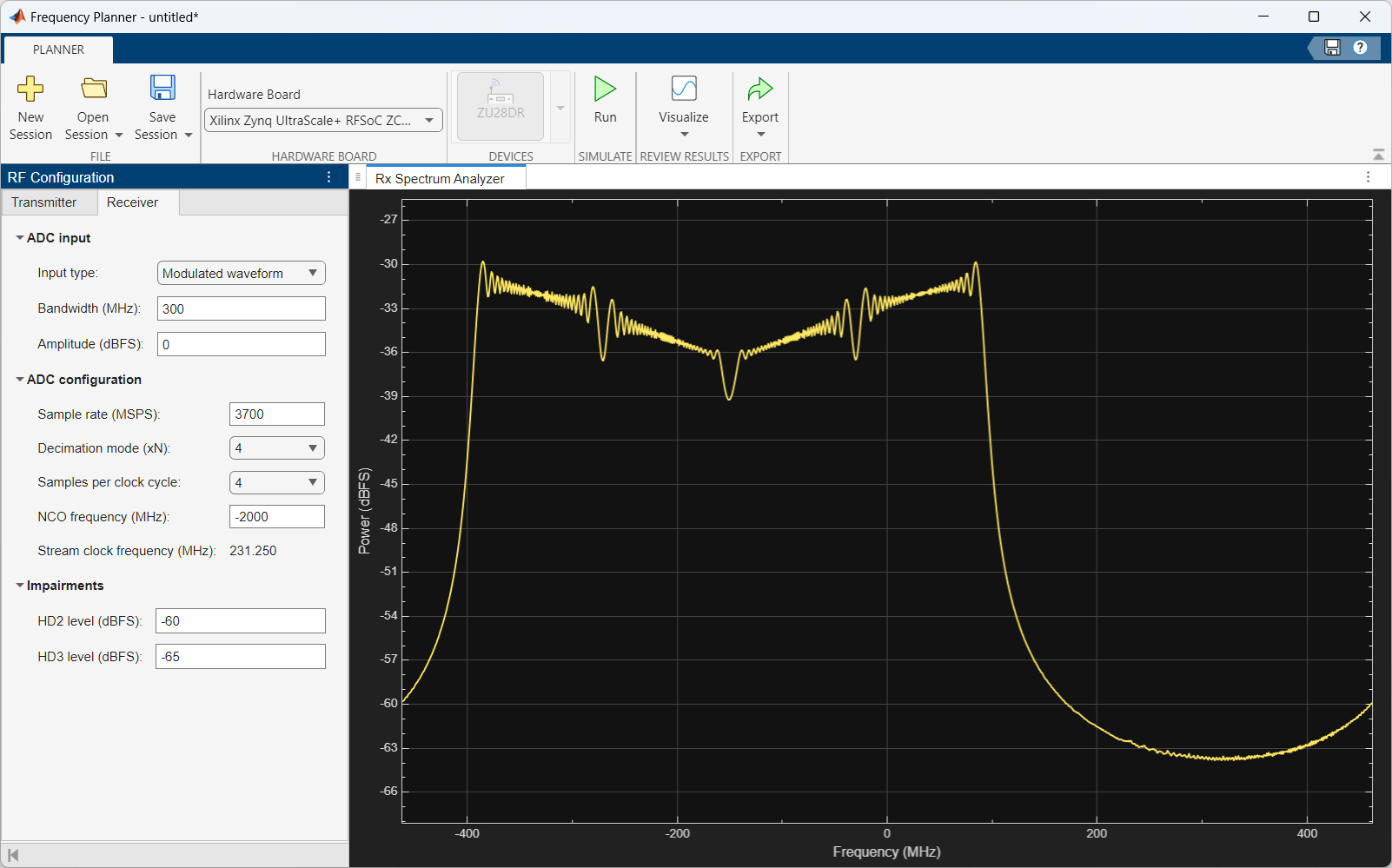
Receive a signal with a bandwidth of 300 MHz, centered at 2000 MHz. Select an ADC sample rate of 3700 MSPS and a decimation mode of 4x. Set the NCO frequency to –2000 MHz.
Signal specifications:
Bandwidth: 300 MHz
RFDC configuration:
ADC sample rate: 3700 MSPS
Decimation mode: 4x
NCO frequency: –2000 MHz
Enter the signal specifications and RFDC configuration in the ADC input and ADC configuration panes in the app. After you select the parameters, click Run to simulate the ADC path. In the Rx Spectrum Analyzer pane, you see that the received signal has distortion, as not all images are discarded.
Solution
To avoid the distortion in the received signal, reduce the ADC sample rate to 3000 MSPS.
Signal specifications:
Bandwidth: 300 MHz
RFDC configuration:
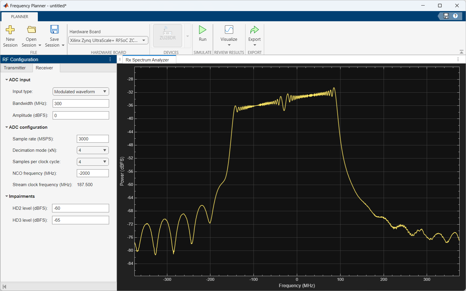
ADC sample rate: 3000 MSPS
Decimation mode: 4x
NCO frequency: –2000 MHz
Enter the signal specifications and RFDC configuration in ADC input and ADC configuration panes in the app. After you select the parameters, click Run to simulate the ADC path. In the Rx Spectrum Analyzer pane, you see that the received signal has no distortion.
Export Configuration of DAC and ADC
To export the configuration of the DAC and ADC as a MAT file, on the Planner tab, from the Export drop-down options, click Export configuration to MAT file.
You can use this MAT file to apply the configuration to an RF Data Converter block. To do so, in the RF Data Converter block mask, on the Frequency Planner tab, click Import configuration.
Conclusion
This example shows how to derive an RFDC configuration based on specific signal requirements using the Frequency Planner app. Using this example as a reference, you can derive and validate your RF configurations for different RFSoC devices.