Waveform Analysis Parameters and Thresholds
The Parallel Link Designer app uses waveform analysis parameters in one of two ways:
To set waveform levels used in waveform and eye diagram processing.
To specify design rule check limits for the app to verify.
All waveform processing extensions are specified in the IBIS files by adding a line that
starts with: |MathWorks. This notation uses the IBIS comment character,
pipe (|), by default. The extensions are not case sensitive. The parameters can be grouped
as:
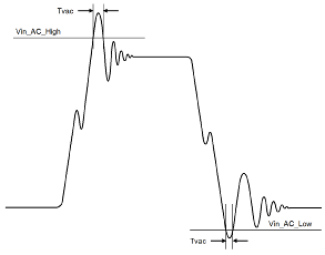
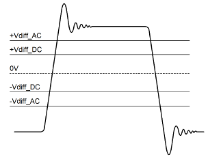
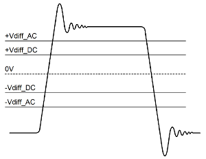
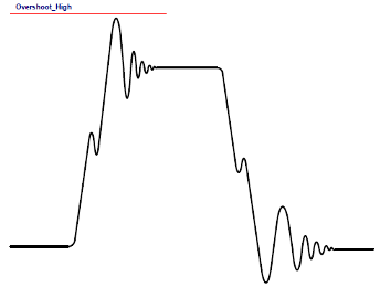
Waveform Processing Parameters: The thresholds used to verify edge transitions (waveform thresholds), the overshoot and area parameters (overshoot thresholds), and the ringback parameters (ringback thresholds). The thresholds are defined for both AC and DC. For more information, see Waveform Processing Parameters.
Waveform Check Parameters: The parameters used to check waveform characteristics. For more information, see Waveform Check Parameters.
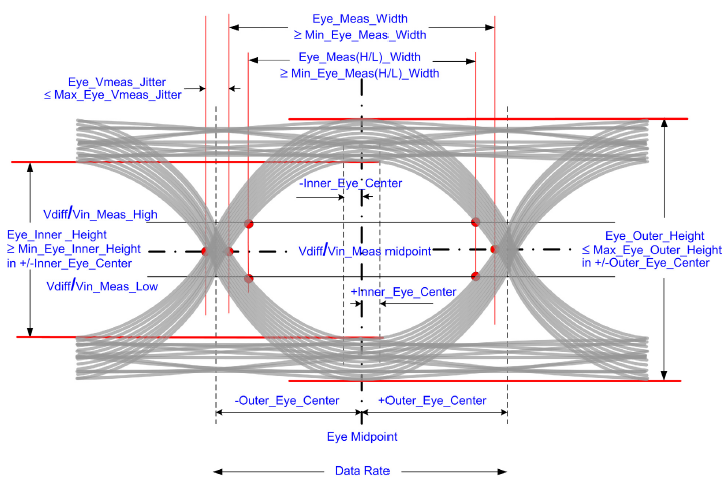
Eye Measurement Parameters: The parameters used to control the eye diagram measurement process. For more information, see Eye Measurement Parameters.
Eye Check Parameters: The parameters that can be used to check the eye diagram parameters. For more information, see Eye Check Parameters.
Etch Delay Measurement Threshold Parameters: The thresholds used to measure etch delays at receivers. For more information, see Etch Delay Measurement Threshold Parameters.
Standard Load Parameters.: The thresholds used to measure the standard load delay on the standard load waveform. For more information, see Standard Load Parameters.
Other Parameters: Other miscellaneous parameters. For more information, see Other Parameters.
Waveform Processing Parameters
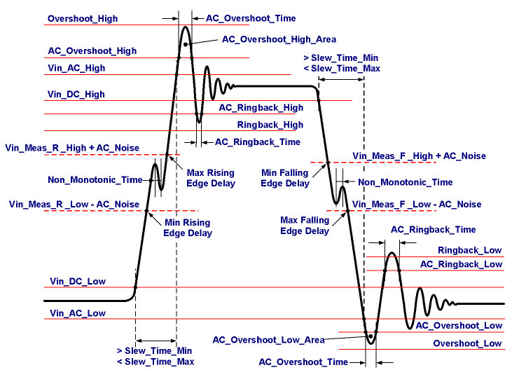
The waveform processing parameters define the waveform edge transitions, overshoots, and ringback thresholds. The thresholds and parameters are:
Waveform Threshold Parameters
These parameters are placed in the [Model Spec] section of the IBIS
file.
| Parameter | Description | Waveform |
|---|---|---|
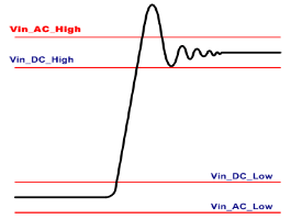
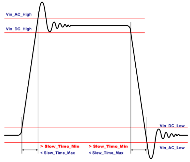
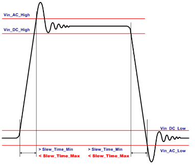
|MathWorks Vin_AC_High |
|
|
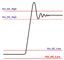
|MathWorks Vin_AC_Low |
|
|
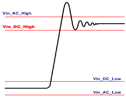
|MathWorks Vin_DC_High |
|
|
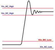
|MathWorks Vin_DC_Low |
|
|
|MathWorks Tvac |
|
|
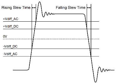
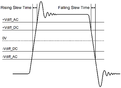
|MathWorks Vdiff_AC |
|
|
|MathWorks Vdiff_DC |
|
|
Overshoot Threshold Parameters
These parameters define the AC and DC overshoots as well as overshoot areas. They are
placed in the [Model Spec] section of the IBIS file.
| Parameter | Description | Waveform |
|---|---|---|
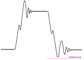
|MathWorks Overshoot_High |
|
|
|MathWorks Overshoot_Low |
|
|
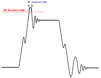
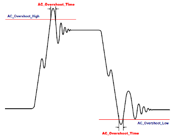
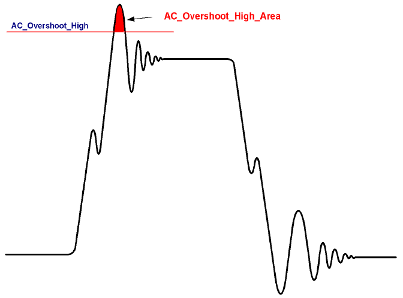
|MathWorks AC_Overshoot_High |
|
|
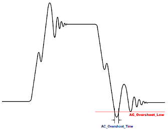
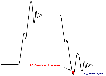
|MathWorks AC_Overshoot_Low |
|
|
|MathWorks AC_Overshoot_Time |
|
|
|MathWorks AC_Overshoot_High_Area |
|
|
|MathWorks AC_Overshoot_Low_Area |
|
|
Ringback Threshold Parameters
These parameters are placed in the [Model Spec] section of the IBIS
file.
| Parameter | Description | Waveform |
|---|---|---|
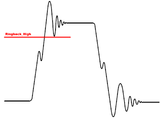
|MathWorks Ringback_High |
|
|
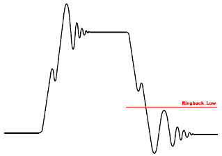
|MathWorks Ringback_Low |
|
|
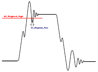
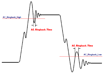
|MathWorks AC_Ringback_High |
|
|
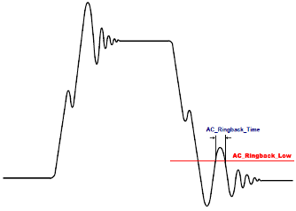
|MathWorks AC_Ringback_Low |
|
|
|MathWorks AC_Ringback_Time |
|
|
Properties of Good Waveform
A proper rising edge has these characteristics:
Starts below
Vin_DC_Low.Never goes below
Overshoot_Lowand does not go belowAC_Overshoot_Lowfor more thanAC_Overshoot_Time.After crossing
Vin_DC_Low, crossesVin_AC_HighbetweenSlew_Time_MinandSlew_Time_Max.Does not ring for more than
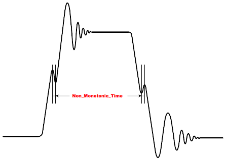
Non_Monotonic_Timewithin the window betweenVin_DC_LowandVin_AC_High.Does not go above
Overshoot_Highand does not go aboveAC_Overshoot_Highfor more thanAC_Overshoot_Time.Does not ring back below
Ringback_Highand does not go belowAC_Ringback_Highfor more thanAC_Ringback_Time.Must end above
Vin_DC_High.
Waveform Check Parameters
The Parallel Link Designer app performs waveform design rule checks as part of the waveform analysis. These checks falls into three categories:
Fatal errors
Quality warnings
Overshoot warnings
The app analyzes the driver and passive I/O buffers only for overshoot. Standard load I/O buffers are only analyzed for timing. Receiver I/O buffers are analyzed for both timing and waveform DRC. Single-ended nodes of differential I/O buffers are analyzed for overshoot. Differential nodes of differential I/O receivers are analyzed for timing and waveform DRC.
Fatal Errors
Fatal errors result into either missing or invalid timing data. Examples of fatal errors include: failed simulation (no transitions at the receiver), insufficient voltage swing at receivers, and ringing clocks. Fatal errors are results of either general simulation setup problems or topology problems (opens in traces or connector models).
Note
The app can generate timing margins even in the presence of fatal waveform errors. For example, if there is only one good data transition and many bad ones, the app reports the timing results on that one good transition and also report the fatal waveform quality errors. So you should always check the waveform analysis log for errors.
| Fatal Error Message | Description/Possible Cause |
|---|---|
| Cannot open waveform data file. | tr0/csd file does not exist. SPICE was
not run or had a fatal error. |
| Output of receiver does not wiggle. | Analyzing receiver at core and core does not have any transitions. Verify that SPICE receiver model does have valid output pin. Verify that the Driver I/O buffer is compatible with the Receiver I/O buffer. Verify that the interconnect subcircuit is properly connected and with proper terminations. |
| Failed to open .prb file. | Internal programming error. |
| Cannot find ibis model. | Internal programming error. |
| Cannot find node. | Internal programming error. Some SPICE formats truncate node names to 16 characters. |
| Cannot find node in simulation file. | Internal programming error. Some SPICE formats truncate node names to 16 characters. |
| Cannot find differential node in simulation file. | Internal programming error. Some SPICE formats truncate node names to 16 characters. |
| Differential driver waveform not identified in simulation file. | Internal programming error. Some SPICE formats truncate node names to 16 characters. |
| Driver waveform not identified in simulation file. | Internal programming error. Some SPICE formats truncate node names to 16 characters. |
| Output of driver does not wiggle. | Driver not operating correctly, or incorrect standard load termination. |
| Driver does not transition. | Driver not operating correctly, or incorrect standard load termination. |
| Driver fails at UI. | Driver does not operate at full range of frequencies analyzed. |
| Simulation has ... transitions; should have... | Internal programming error. |
| No receiver transitions. | Signal at receiver does not transition through (VinL+VinH)/ 2. Open in subcircuit between driver and receiver. Improper termination. Mismatched driver and receiver models. |
| Cannot match stimulus with node. | Receiver transitions, but waveform is problematic. |
| No receiver transition for stimulus transition at... | May have timing data for some transitions, not all. |
| No receiver transition in analysis window. | May have timing data for some transitions, not all. |
| No standard load transition in analysis window. | Timing not corrected for standard loads. |
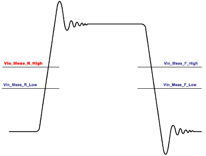
Clock rings through Vin_Meas_R_High. | Rising clock edge rings through Vin_Meas_R_High. Possible
double clocking. |
Clock rings through Vin_Meas_F_Low. | Falling clock edge rings through Vin_Meas_F_Low. Possible
double clocking. |
Clock rings through Vdiff. | Rising clock rings through +Vdiff. Falling clock rings
through –Vdiff. Possible double clocking. |
Quality Warnings
Quality warnings indicate that the app generated timing data, but the timing results may be incorrect because the shape of the waveform transition is outside of manufactures specifications: Examples of quality warnings include slow slew rates and ringing data. Waveform quality warnings fall into these categories:
Eye rule violations
Miscellaneous edge rule violations
Ringback rule violations
Initial and final state rule violations
AC rules violations
Bus turnaround violations
Note
Bus turnaround waveform analysis only pattern matches the initial priming edges. After the first bus turnaround, the waveform analysis at receivers is done in an analysis window determined by the stimulus edges and a time offset calculated during the analysis of the priming edges.
| Waveform Quality Warning | Affects Margin? | Description/Possible Causes |
|---|---|---|
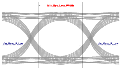
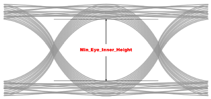
| Min Eye Inner Height | Yes | Eye Inner Height < rule (Min_Eye_Inner_Height). |
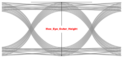
| Max Eye Outer Height | Yes | Eye Outer Height > rule (Max_Eye_Outer_Height). |
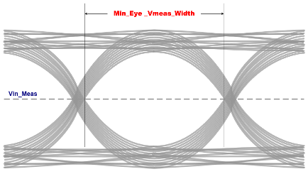
Min Eye VinMeas Width | Yes | Eye width (measured at inside tear ducts) < rule
(Min_Eye_Vmeas_Width). |
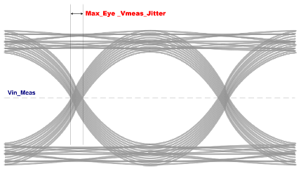
Max Eye VinMeas Jitter | Yes | Eye tear duct width > rule (Max_Eye_Vmeas_Jitter). |
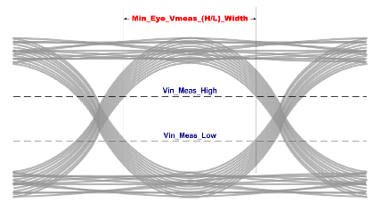
Min Eye VinMeas(H/L) Width | Yes | Eye inter width measured at VinMeas < rule
(Min_Eye_Vmeas(H/ L)_Width). |
| Slew Time Max | Yes | Slew time > rule (Slew_Time_Max). |
| Slew Time Min | Yes | Slew time < rule (Slew_Time_Min). |
| Non-Monotonic | No | Rising edge is falling for more than Non_monotonic_time
during transition. Falling edge is rising for more than
Non_monotonic_time during transition. |
| Data rings through | No | Rising data edge rings through Vin_Meas_R_High. Falling
data edge rings through Vin_Meas_F_Low. |
Data rings through Vdiff | No | Rising data edge rings through +Vdiff. Falling data edge
rings through –Vdiff. |
| Ringback High | Yes | Rising edge goes above Vin_AC_High then below
Ringback_High then above Vin_DC_High.
Falling edge goes below Vin_DC_High then below
Ringback_High then above
Vin_DC_High. |
| Ringback Low | Yes | Falling edge goes below Vin_AC_Low then above
Ringback_Low then below Vin_DC_Low. Rising
edge goes above Vin_DC_Low then above
Ringback_Low then above
Vin_DC_Low. |
| AC Ringback High | Yes | Rising edge goes above Vin_AC_High then below
AC_Ringback_High for more than
AC_Ringback_Time then above Vin_DC_High.
Falling edge goes below Vin_DC_High then below
AC_Ringback_High for more than
AC_Ringback_Time then above
Vin_DC_High. |
| AC Ringback Low | Yes | Falling edge goes below Vin_AC_Low then above
AC_Ringback_Low for more than
AC_Ringback_Time then below Vin_DC_Low.
Rising edge goes above Vin_DC_Low then above
AC_Ringback_Low for more than
AC_Ringback_Time then below
Vin_DC_Low. |
Vin_Meas_High + AC_Noisegreater than
Ringback_High | Yes | Ringback rules are disabled when the ringback voltage crosses the
VinMeas voltages when adjusted for
AC_Noise. Generated once per transfer net receiver. |
Vin_Meas_Low – AC_Noise less than
Ringback_Low | Yes | Ringback rules are disabled when the ringback voltage crosses the
VinMeas voltages when adjusted for
AC_Noise. Generated once per transfer net receiver. |
Initial state above Vin_DC_Low | Yes | Rising edge starts above Vin_DC_Low. |
Initial state below Vin_DC_High | Yes | Falling edge starts below Vin_DC_High. |
Initial state below Vdiff_DC | Yes | Edge starts below Vdiff_DC. |
Initial state below Vdiff | Yes | Edge starts below Vdiff. |
Initial state above (Vin_Meas_R_Low –
AC_Noise) | Yes | Rising edge starts above (Vin_Meas_R_Low –
AC_Noise) |
Initial state below (Vin_Meas_F_High +
AC_Noise) | Yes | Falling state starts below (Vin_Meas_F_High +
AC_Noise) |
Initial state within AC Noise of Vdiff | Yes | Edge starts within AC Noise of Vdiff. |
Final state above Vin_DC_Low | Yes | Falling edge above Vin_DC_Low. |
Final state below Vin_DC_High | Yes | Rising edge below Vin_DC_High. |
Final state below Vdiff_DC | Yes | Edge ends below Vdiff_DC. |
Final state below Vdiff | Yes | Edge ends below Vdiff. |
Final state below (Vin_Meas_R_High +
AC_Noise) | Yes | Rising edge below (Vin_Meas_R_High +
AC_Noise) |
Final state above (Vin_Meas_F_Low –
AC_Noise) | Yes | Falling edge above (Vin_Meas_F_Low –
AC_Noise) |
Final state within AC Noise of Vdiff | Yes | Edge ends within AC Noise of Vdiff. Max timing is the end
of the analysis window. |
Enters transition but ends below (Vin_Meas_R_High +
AC_Noise) | Yes | Rising edge crosses Vin_Meas_R_Low –
AC_Noise but ends below Vin_Meas_R_High +
AC_Noise. Maximum timing is end of analysis window. |
Enters transition but ends above (Vin_Meas_F_Low –
AC_Noise) | Yes | Falling edge crosses Vin_Meas_F_High +
AC_Noise but ends above Vin_Meas_F_Low –
AC_Noise. Maximum timing is the end of the analysis
window. |
Did not enter transition and ends below (Vin_Meas_R_High +
AC_Noise) | Yes | Falling edge never crosses Vin_Meas_F_High +
AC_Noise but ends below (Vin_Meas_R_High +
AC_Noise). Minimum timing is the start of the analysis
window. |
Did not enter transition and ends above (Vin_Meas_F_Low –
AC_Noise) | Yes | Rising edge never crosses Vin_Meas_R_Low –
AC_Noise but ends above Vin_Meas_R_High +
AC_Noise. Minimum timing is the start of the analysis
window. |
Did not cross Vin_Meas_R_High | Yes | Rising edge did not cross Vin_Meas_R_High. |
Did not cross Vin_Meas_F_Low | Yes | Falling edge did not cross Vin_Meas_F_Low. |
Did not exit Vdiff range | Yes | Rising edge started below –Vdiff but never crossed
+Vdiff. Falling edge started above +Vdiff
but never crossed –Vdiff. |
Did not cross Vdiff_AC | Yes | Edge did not cross Vdiff_AC. |
Did not cross Vin_AC_High | Yes | Rising edge not cross Vin_AC_High. |
Did not cross Vin_AC_Low | Yes | Falling edge did not cross Vin_AC_Low. |
Final state above Vin_Meas_F_Low | Yes | Low level final state above Vin_Meas_F_Low. |
Final state below Vin_Meas_R_High | Yes | High level final state below Vin_Meas_R_High. |
Overshoot Warnings
Overshoot warnings indicate potential component reliability and failure problems. Overshoot at drivers or receivers can affect the reliability and lifetime of components.
| Waveform Overshoot Warning | Affects Timing Margin? | Description/Possible Cause |
|---|---|---|
| Overshoot High | No | Signal goes above Overshoot_High. |
| Overshoot Low | No | Signal goes below Overshoot_Low. |
| AC Overshoot High | No | Signal goes above AC_Overshoot_High for more than
AC_Overshoot_Time. |
| AC Overshoot Low | No | Signal goes below AC_Overshoot_Low for more than
AC_Overshoot_Time |
Note
Overshoot_High and AC_Overshoot_High warnings
can either have just a TT (typ) value or values for all three (typical, fast, and slow)
process corners. If the warnings just have the typical values, then the level is
adjusted by the difference between the model rail voltage and the actual rail voltage
used in the simulation.
Waveform Check Parameters
These parameters check the edges of the processed waveforms. They are placed in the
[Model
          Spec]
section of the IBIS file.
| Parameter | Description | Waveform |
|---|---|---|
|MathWorks Slew_Time_Min |
Note If using |
|
|MathWorks Slew_Time_Max |
Note If using |
|
|MathWorks Nonmonotonic_time |
|
|
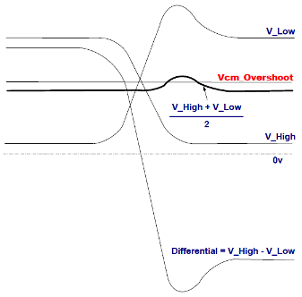
|MathWorks Vcm_overshoot |
|
|
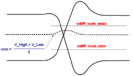
|MathWorks Vdiff_Vcm_min/max |
|
Eye Measurement Parameters
These parameters control how the Parallel Link Designer app measures the eye
diagram parameters. They are placed in the [Model Spec] section of the
IBIS file.
| Parameter | Description | Waveform |
|---|---|---|
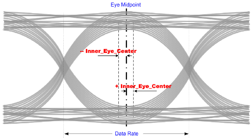
|MathWorks Inner_Eye_Center |
|
|
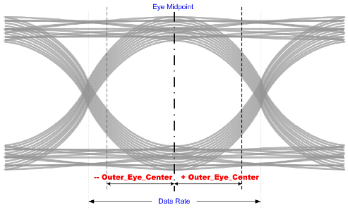
|MathWorks Outer_Eye_Center |
|
|
Eye Check Parameters
These parameters are used to check the eye that the Parallel Link Designer
app calculates from the waveform data. They are placed in the [Model
Spec] section of the IBIS file. The app reports the violations of these
parameters in the Waveform Quality tab of the Waveform and Timing
Report window.
| Parameter | Description | Waveform |
|---|---|---|
|MathWorks Max_Eye_Vmeas_Jitter |
|
|
|MathWorks Min_Eye_Vmeas_Width |
|
|
|MathWorks Min_Eye_Vmeas(H/L)_Width |
|
|
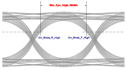
|MathWorks Min_Eye_High_Width |
|
|
|MathWorks Min_Eye_Low_Width |
|
|
|MathWorks Max_Eye_Outer_Height |
|
|
|MathWorks Min_Eye_Inner_Height |
|
|
Etch Delay Measurement Threshold Parameters
The Parallel Link Designer app measures the minimum and maximum raw etch delays on the rising and falling edges of the waveform. To calculate the final etch, the app subtracts the standard load delay from the derated raw etch delay. The app can measure the delays on either single-ended waveforms or differential waveforms.
Single-Ended Etch Delay
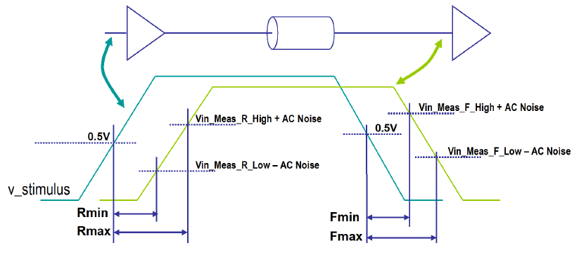
Single-ended raw etch delays are measured on single-ended waveforms. The delay measurement is different in non-STAT mode and STAT mode.
Non-STAT Mode Single-Ended Raw Etch Delay Measurements
STAT Mode Single-Ended Raw Etch Delay Measurements
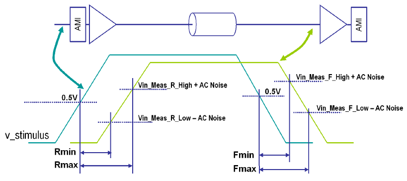
For non-STAT mode simulations, every edge of every waveform is measured except for skipped edges. The first and last edge of every waveform are skipped by default. The receiver thresholds used for each delay are dependent on the target probe points:
| Raw Etch Delay | Target Probe Point | Target Measurement Threshold |
|---|---|---|
| Rmin (Rising minimum) | pad | Vin_Meas_R_Low |
| pin | Vin_Meas_R_Low | |
| core | 20% voltage on z node | |
| Rmax (Rising maximum) | pad | Vin_Meas_R_High |
| pin | Vin_Meas_R_High | |
| core | 80% voltage on z node | |
| Fmin (Falling minimum) | pad | Vin_Meas_F_High |
| pin | Vin_Meas_F_High | |
| core | 80% voltage on z node | |
| Fmax (Falling maximum) | pad | Vin_Meas_F_Low |
| pin | Vin_Meas_F_Low | |
| core | 20% voltage on z node |
The z node is the output of the receiver buffer (the chip side of the buffer)
For STAT Mode simulations, use the parameter Waveform Analysis Bits from the Simulation Parameter dialog box to specify the number of edges to measure. The target probe point is always pad by default.
To account for the timing affect of the noise, these thresholds are offset by the AC noise parameter. The actual measurement point used for each of the thresholds are:
| Threshold | Actual Measurement Point |
|---|---|
Vin_Meas_R_Low | Vin_Meas_R_Low – AC noise |
Vin_Meas_R_High | Vin_Meas_R_High + AC noise |
Vin_Meas_F_High | Vin_Meas_F_High + AC noise |
Vin_Meas_F_Low | Vin_Meas_F_Low – AC noise |
The _Low thresholds become lower and the _High
thresholds become higher when the AC noise is greater than zero. This makes the minimum
delays shorter and the maximum delays longer, which reduces timing margins.
Differential Etch Delay
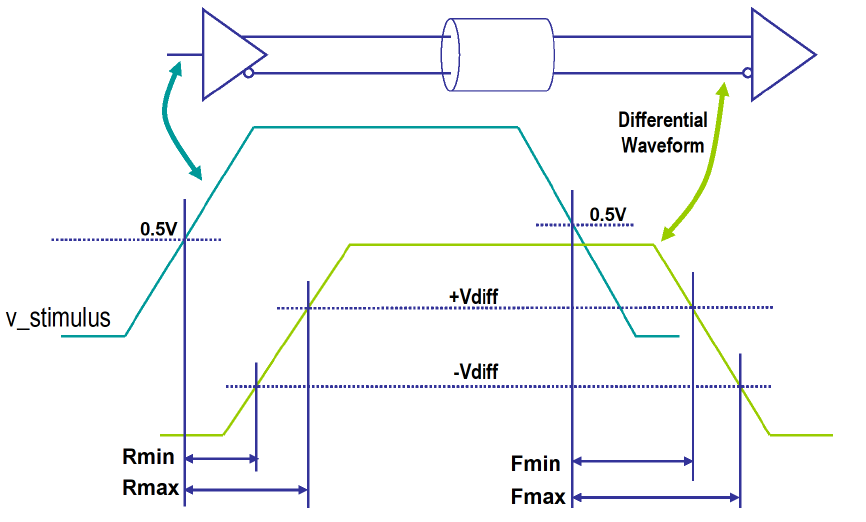
The app measures the differential raw etch delays on the differential waveform (non-inverting minus inverting). The delay measurement is different in non-STAT mode and STAT mode.
Non-STAT Mode Differential Raw Etch Delay Measurements
STAT Mode Differential Raw Etch Delay Measurements
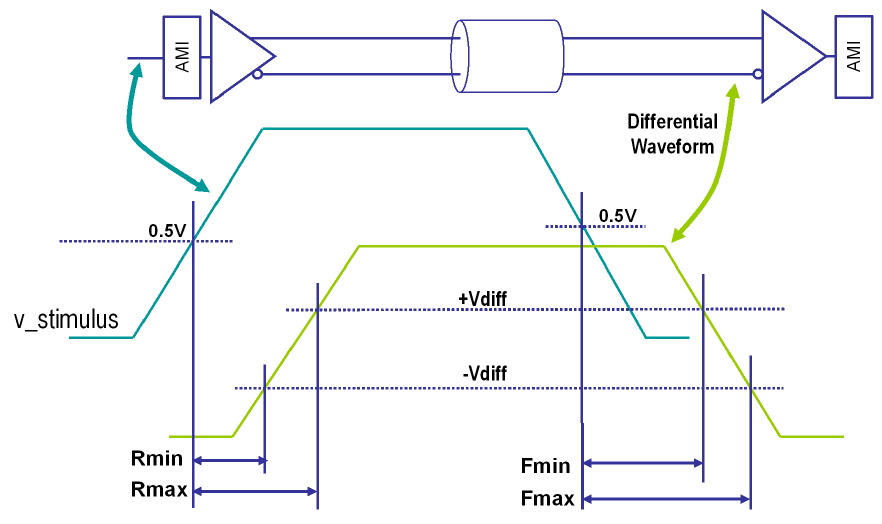
For non-STAT mode simulations, every edge of every waveform is measured except for skipped edges. The first and last edge of every waveform are skipped by default. The receiver thresholds used for each delay are dependent on the target probe points:
| Raw Etch Delay | Target Probe Point | Target Measurement Threshold |
|---|---|---|
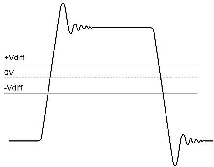
| Rmin (Rising minimum) | pad | -Vdiff |
| pin | -Vdiff | |
| core | 50% voltage on z node | |
| Rmax (Rising maximum) | pad | +Vdiff |
| pin | +Vdiff | |
| core | 50% voltage on z node | |
| Fmin (Falling minimum) | pad | +Vdiff |
| pin | +Vdiff | |
| core | 50% voltage on z node | |
| Fmax (Falling maximum) | pad | -Vdiff |
| pin | -Vdiff | |
| core | 50% voltage on z node |
The z node is the output of the receiver buffer (the chip side of the buffer).
For STAT Mode simulations, use the parameter Waveform Analysis Bits from the Simulation Parameter dialog box to specify the number of edges to measure. The target probe point is always pad by default.
AC Noise does not affect differential etch delays.
Etch Delay Parameters
These parameters are placed in the [Model Spec] section of the IBIS
file.
| Parameter | Description | Waveform | ||||||||||
|---|---|---|---|---|---|---|---|---|---|---|---|---|
|MathWorks Vin_Meas_R_High |
|
| ||||||||||
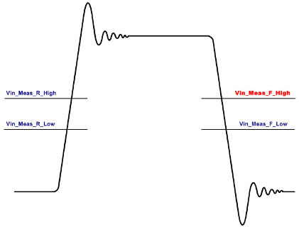
|MathWorks Vin_Meas_F_High |
|
| ||||||||||
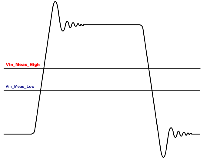
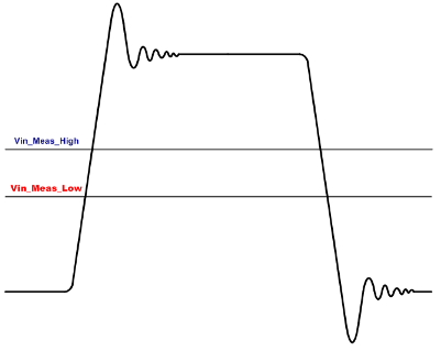
|MathWorks Vin_Meas_High |
|
| ||||||||||
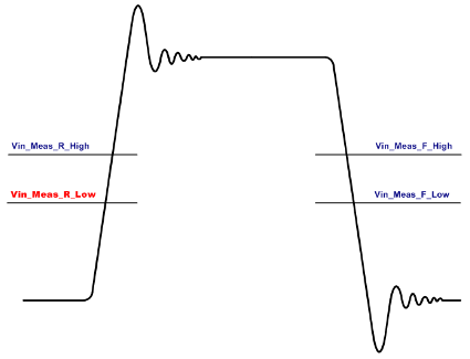
|MathWorks Vin_Meas_R_Low |
|
| ||||||||||
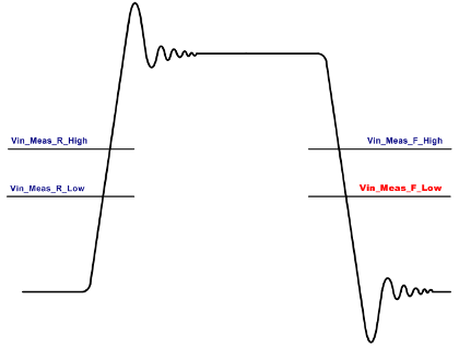
|MathWorks Vin_Meas_F_Low |
|
| ||||||||||
|MathWorks Vin_Meas_Low |
|
| ||||||||||
|MathWorks vdiff |
|
| ||||||||||
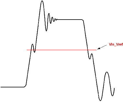
|MathWorks Vin_Vref |
|
| ||||||||||
|MathWorks Derate_* |
| |||||||||||
|MathWorks Derate Slew |
|
Standard Load Parameters
| Parameter | Description |
|---|---|
|MathWorks VmeasR |
|
|MathWorks VmeasF |
|
|MathWorks VmeasRef |
|
Other Parameters
|MathWorks Probe_Points Parameter
The Parallel Link Designer app uses the |MathWorks
Probe_Points to override the transfer net probe point property for a model.
The parameter also specifies the probe point to use for the model. The parameter is set in
the [Model] section of the IBIS buffer model.
Format: |MathWorks Probe_Points <drv>/<rcv>, where
<drv> is one of the sl_pin,
sl_pad, or core and <drv>
is one of the pin, pad, or
core.
STAT Mode Parameters
The Parallel Link Designer app uses the STAT mode parameters to apply an eye mask during the STAT Mode post-processing. The app reports the margins in the Statistical and Time Domain tabs of the Results. The parameters are:
|MathWorks Skew_Eye_Latch— Applies an eye mask at the latch (after equalization).|MathWorks Skew_Eye_Pad— Applies an eye mask at the die pad (before equalization).
Threshold Parameter Precedence
| Threshold Name | Parameters (Highest Precedence First) | Qualifier | Corner Used |
|---|---|---|---|
Overshoot_High | |MathWorks Overshoot_High | typ min max | |
D Overshoot_High | If S Overshoot_High is defined | typ min max typ | |
S Overshoot_High | typ min max typ | ||
Overshoot_Low | |MathWorks Overshoot_Low | typ min max | |
D Overshoot_Low | If S Overshoot_Low is defined | typ min max typ | |
S Overshoot_Low | typ min max typ | ||
AC_Overshoot_High | |MathWorks AC_Overshoot_High | typ min max | |
S AC_Overshoot_High | If D_Overshoot_High is defined | typ min max typ | |
AC_Overshoot_Low | |MathWorks AC_Overshoot_Low | typ min max | |
S AC_Overshoot_Low | If D_Overshoot_Low is defined | typ min max typ | |
AC_Overshoot_Time | |MathWorks AC_Overshoot_Time | typ | |
D AC_Overshoot_Time | typ | ||
AC_Overshoot_High_Area | |MathWorks AC_Overshoot_High_Area | typ min max | |
AC_Overshoot_Low_Area | |MathWorks AC_Overshoot_Low_Area | typ min max | |
VmeasR | |MathWorks VmeasR | typ min max | |
|MathWorks Vmeas | typ | ||
Vmeas | |||
VmeasF | |MathWorks VmeasF | typ min max | |
|MathWorks Vmeas | typ | ||
Vmeas | |||
Vin_Meas_R_High | |MathWorks Vin_Meas_R_High | typ min max | |
|MathWorks Vin_Meas_High | typ min max | ||
Vth_Max + Offset | typ min max | ||
Vth + Offset | typ min max | ||
Vin_DC_High | typ min max | ||
Vin_AC_High | typ min max | ||
VinH | typ min max | ||
Vin_Meas_F_High | |MathWorks Vin_Meas_F_High | typ min max | |
|MathWorks Vin_Meas_High | typ min max | ||
Vth_Max + Offset | typ min max | ||
Vth + Offset | typ min max | ||
Vin_DC_High | typ min max | ||
Vin_AC_High | typ min max | ||
VinH | typ min max | ||
Vin_Meas_R_Low | |MathWorks Vin_Meas_R_Low | typ min max | |
|MathWorks Vin_Meas_Low | typ min max | ||
Vth_Min + Offset | typ min max | ||
Vth + Offset | typ min max | ||
Vin_DC_Low | typ min max | ||
Vin_AC_Low | typ min max | ||
VinL | typ min max | ||
Vin_Meas_F_Low | |MathWorks Vin_Meas_F_Low | typ min max | |
|MathWorks Vin_Meas_Low | typ min max | ||
Vth_Min + Offset | typ min max | ||
Vth + Offset | typ min max | ||
Vin_DC_Low | typ min max | ||
Vin_AC_Low | typ min max | ||
VinL | typ min max | ||
Vin_AC_High | |MathWorks Vin_AC_High | typ min max | |
Vinh_ac + Vth + Offset | typ | ||
VinH | typ min max | ||
Vin_AC_Low | |MathWorks Vin_AC_Low | typ min max | |
Vinl_ac + Vth + Offset | typ | ||
VinL | typ min max | ||
Vin_DC_High | |MathWorks Vin_DC_High | typ min max | |
Vinh_dc + Vth + Offset | typ | ||
VinH | typ min max | ||
Vin_DC_Low | |MathWorks Vin_DC_Low | typ min max | |
Vinl_dc + Vth + Offset | typ | ||
VinL | typ min max | ||
Vdiff | |MathWorks Vdiff | ||
[Diff Pin] vdiff | Pre-layout: max vdiff of all pin pairs that use the
model | ||
| 0.2V | |||
Vdiff_DC | |MathWorks Vdiff_DC | ||
Vdiff | |||
[Diff Pin] vdiff | Pre-layout: max vdiff of all pin pairs that use the
model | ||
| 0.2V | |||
Vdiff_AC | |MathWorks Vdiff_AC | ||
Vdiff_DC | |||
Vdiff | |||
[Diff Pin] vdiff | Pre-layout: max vdiff of all pin pairs that use the
model | ||
| 0.2V | |||
Slew_Time_max | |MathWorks Slew_Time_Max | typ | |
|MathWorks Tslew_ac | typ | ||
|MathWorks Tdiffslew_ac | typ | ||
Slew_Time_min | |MathWorks Slew_Time_Min | typ | |
Ringback_High | |MathWorks Ringback_High | typ min max | |
Vin_DC_High | typ min max | ||
VinH | typ min max | ||
Ringback_Low | Ringback_Low | typ min max | |
Vin_DC_Low | typ min max | ||
VinL | typ min max | ||
AC_Ringback_High | AC_Ringback_High | typ min max | |
AC_Ringback_Low | AC_Ringback_Low | typ min max | |
AC_Ringback_Time | AC_Ringback_Time | typ | |
Vin_Vref (Rising Edge) | Vin_Vref | typ min max | |
(Vin_Meas_R_High +
Vin_Meas_R_Low)/2 | typ min max | ||
Vin_Vref (Falling Edge) | Vin_Vref | typ min max | |
(Vin_Meas_F_High +
Vin_Meas_F_Low)/2 | typ min max | ||
Vdiff_vcm_min | Vdiff_vcm_min | typ | |
Vcross_low | typ | ||
Vdiff_vcm_max | Vdiff_vcm_max | typ | |
Vcross_high | typ |
Note
Overshoot voltage corner usage: When the I/O corner voltages setting is Scale IBIS Model [Voltage Range] Typical Value in the Simulation Preferences, the typ value is used and scaled. When the I/O corner voltages setting is Use IBIS Model [Voltage Range] in the Simulation Preferences, the typ, min, and max values are used.
Note
