DDRx Timing and Waveform Mask Analysis
This example shows how to use the Parallel Link Designer app to perform timing analysis for the DDR (Double Data Rate) family of memory interface protocols. You can use either Setup and Hold margins or by waveform eye-diagram compliance masks to perform the timing analysis. The DDR Memory Down (DDR4_MD) example kit uses both timing and waveform mask analysis. Specifically for DDR4 systems, timing analysis is performed on clock-address/command interface, and waveform compliance masks are applied to strobe-data(DQS-DQ) interface. Other DDR types may use only timing analysis, or only waveform mask analysis or a blend depending on individual standards.
Timing and Waveform Analysis Overview
Timing and Waveform Mask Analysis are used in signal integrity analysis of a parallel link system. This tutorial shows how Parallel Link Designer can be used to analyze a DDR memory interface using a DDR4 implementation kit as the starting point. This example assumes you are referencing the "DDR4_MD" kit, which allows you to begin signal Integrity analysis immediately since all models and schematic sheets are part of the kit. You can import a new IBIS (.ibs) file for an example SDRAM and see how it references Timing (.tmg) and Include (.inc) files for margin analysis by the Parallel Link Designer app. If an implementation kit were not available for this interface, you would need to build the simulation environment (Parts, IBIS Models, and pre-layout topologies) from a new project. After showing you how to import a new IBIS SDRAM part, this example also illustrates some of the steps involved in setting up Timing and Include files to enable timing and waveform mask analysis.
DDR4 Memory-Down Kit
Signal Integrity Toolbox™ kits are an easy way to jumpstart your analysis by providing an interface that is completely configured and ready to simulate. You can customize the kits by adding models and modifying parameter values for your specific implementation. This example shows you how to import a new IBIS file for an SDRAM, then modify a Timing (.tmg) file and Include (.inc) file to enable Timing and Waveform Mask analysis in the Parallel Link Designer app. The accompanying kit is already configured with details such as clock domain, transfer net configuration, and sheets classified as Data, Clock, and Strobe as appropriate for a DDR4 interface.
Open the DDR4_MD kit in the Parallel Link Designer app using the openSignalIntegrityKit function.
openSignalIntegrityKit("DDR4_MD");
Then you can download the attached file "ex_sdram_x6.zip" and unarchive to a temporary folder. The contents of this archive are as follows:
IBIS file representing an imagined "x6 SDRAM" for the purposes of this example
Include files to configure logic thresholds and eye masks for Waveform Analysis
A Timing file to place in your project folder "DDR4_MD\si_lib\timing"
Import IBIS File and Reconfigure Sheets
You can import the IBIS file "ex_sdram_x6.ibs" by clicking on the "Libraries->Import IBIS..." menu from the toolbar. You can see in your OS file exlporer that the IBIS (.ibs) file is placed in the folder "DDR4_MD\si_lib\ibis" along with Include (.inc) files called within the IBIS file.

Next, place the file "ex_sdram_x6.tmg" in your project folder "DDR4_MD\si_lib\timing" where this is the Timing file used by Parallel Link Designer to simulate with the IBIS file "ex_sdram_x6.ibs." The contents of the Timing file as well as the Include files will be explained in the following sections.
Timing Analysis Configuration
This section describes the Transfer Net and timing model requirements for various types of timing.
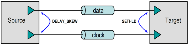
Source-Synchronous Timing
You can see in the figure below an illustration of Source-Synchronous data transfer timing elements that could represent, for this kit example, a DDR memory interface. The figure shows a data net with its associated clock net and is used to describe requirements to configure a Source-Synchronous interface for timing analysis.

Source-Synchronous analysis has the following configuration requirements:
You must create or configure the appropriate Transfer Net schematic sheets. In the simplest case, there must be two schematic sheets, one for the data net and one for the clock net. The data schematic sheet should be of type Data and the clock schematic sheet should be of type Clock or Strobe. Because you have a kit already configured with these sheets, you can do this in the kit by clicking on the SDRAM parts on each sheet and changing the IBIS File to "ex_sdram_x6.ibs".

Then you can select the Address/Command pins for the "ex_sdram_x6.ibs" model:

The Project Parts must have Timing Models. Each timing model must have a SETHLD (Setup and Hold) timing constraint defined between the data and clock PINDEF groups. You must also add a DELAY_SKEW statement in the timing model for the driving chip between the data and clock PINDEF groups. However, for this example a Timing file has been provided, and will be discussed in more detail below.
Note: You should already have placed the file "ex_sdram_x6.tmg" in your project folder ("DDR4_MD\si_lib\timing").
Configure Include Files for Waveform Analysis
This example will next show you where the thresholds for Waveform Analysis are configured in the Include file, and where the Compliance Mask is defined as well.
Note: Within IBIS, Timing, and Include files, you may notice the following keyword with an argument following it:
|MathWorks <argument> <parameter>...
This would normally be considered an IBIS comment line (due to the pipe character, "|") but is in fact is a keyword to flag the parser within Parallel Link Designer to configure a parameter specified by the argument provided. For example, logic thresholds for the DDR4 standard would be defined for an SDRAM IBIS [Model] for Address/Command as follows in the Include file "ex_add_ctrl_sstl_12.inc." For more information, see Waveform Analysis Parameters and Thresholds.
Parameters in Include file for Waveform Analysis
| TYP MIN MAX
|| Based on VDDQ: 1.2 1.14 1.26
|MathWorks Overshoot_High 1.5 1.44 1.56
|MathWorks AC_Overshoot_High 1.2 1.14 1.26
|MathWorks Vin_AC_High 0.700 0.670 0.730
|MathWorks Vin_Meas_R_High 0.700 0.670 0.730
|MathWorks Vin_Meas_F_High 0.675 0.645 0.705
|MathWorks Vin_DC_High 0.675 0.645 0.705
|MathWorks Vin_DC_Low 0.525 0.495 0.555
|MathWorks Vin_Meas_R_Low 0.525 0.495 0.555
|MathWorks Vin_Meas_F_Low 0.500 0.470 0.530
|MathWorks Vin_AC_Low 0.500 0.470 0.530
|MathWorks AC_Overshoot_Low 0.0 0.0 0.0
|MathWorks Overshoot_Low -0.3 -0.3 -0.3
|MathWorks Slew_Time_Min 25ps
|MathWorks Slew_Time_Max 175ps
|
||Standard load measurement level
|MathWorks Vmeas 0.600 0.570 0.630
|
||Standard load termination value
|MathWorks Vref 1.2 1.14 1.26
There are a few other parameters you will want to enable Eye Mask Compliance for DDR4 or DDR5 or as appropriate for your interface. For example, in the DATA class DQ Include file you would set the following:
||| DDR4/5 specific timing parameters:
|
|| Enable eye mask processing on receivers:
|| YES = DDR Eye Mask analysis done.
|| No (Default) = No DDR4/5 analysis done.
|MathWorks MaskAnalysis YES
|
|| Which Vref to use for analysis on receivers:
|| YES = Use IBIS levels relative to Floating Vref
|| No (Default) = Use fixed Vref as defined by Vin_vref
|MathWorks FloatingVref YES
|
|| Granularity for Mask Analysis
|| YES = Do Mask Analysis Per Pin
|| No (Default) = Do Mask Analysis Per Bundle
|MathWorks MaskPerPin Yes
|
|| Which Thresholds to use for Timing Analysis
|| YES = Use Vref +/- (ViVW_Total/2)
|| No (Default) = Use IBIS Model thresholds
|MathWorks TimingViVW Yes
Configure Include Files for Waveform Mask Analysis
Parameters in Include file to configure Eye Mask analysis
Here you can see a plot of the mask defined in the DATA class DQ Include file you would set the following at the section for a clock period of 0.938:
Note: The parameters ViVW_Total, TiVW_Total, and TiVW_Output_Skew are defined in the DDR4 or DDR5 standard (JESD79-4 and JESD79-5, respectfully), you can refer to those as appropriate for their definitions and more details about them.
|MathWorks elseif ( $clock_domain(ddr4_ck_period)==0.938)
Where the following statements configure the parameters AC_Overshoot_High_Area and Low_Area for this data rate:
|| PLD Waveform Quality and Timing Levels for DDR4-2133
|MathWorks AC_Overshoot_High_Area 0.0901 0.0901 0.0901
|MathWorks AC_Overshoot_Low_Area 0.0788 0.0788 0.0788
And where the following configure the Mask for Eye-Diagram compliance and margin calculations for this data rate:
|MathWorks TiVW_Total 0.094ns 0.094ns 0.094ns
|MathWorks TiPW 0.272ns 0.272ns 0.272ns
|| Set SDRAM output skew to 0.4UI (DQ_SKEW_MAX - DQ_SKEW_MIN)
|MathWorks TiVW_Output_Skew 0.188ns
|MathWorks SRIN_diVW_Min 1.0
|MathWorks SRIN_diVW_Max 9.0
Run Simulation and View Results
After you run the simulation for Clock, Address/Command, Strobe and Data signals, you can evaluate margins for this DDR4 interface using the imagined "x6" SDRAM model deck. You can do this in Signal Integrity Viewer, which has many plot functions available to assist you in analyzing Waveforms and Eye Masks. You can see the result by plotting a Waveform for an Address-Command transaction where the Receiver is "ddr4_sdram_0," then find the appropriate row in the results table of the Signal Integrity Viewer, right-click to open the Show Waveform dialog and select At Target Pad.
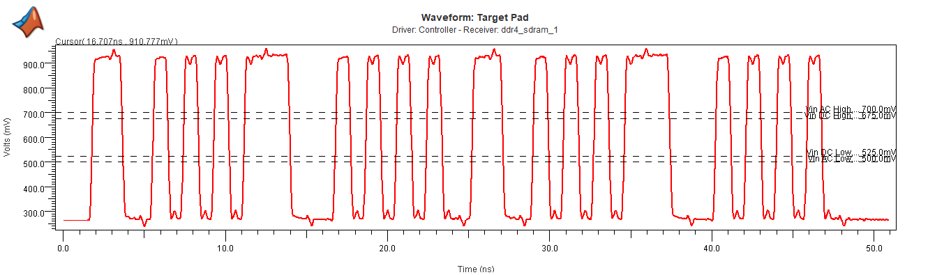
You can see the result by plotting an Eye Diagram for a Data Write transaction where the Receiver is "ddr4_sdram_0," you can find the appropriate row in the results table of the Signal Integrity Viewer, right-click to open the Show Waveform dialog and select At Target Pad.

Configure Timing Files for Timing Analysis
PARAMS: Section of Timing File
In the Timing file, you can see there are multiple sections. The first section is the PARAMS: section, where you can see timing margins are defined for DDR4-2133 (clock period 0.938, DQ bit time 0.469).
PARAMS:
<...>
# DDR4-2133
elseif (DQ_BIT_TIME==0.469)
ADDCMD_SETUP = 0.080
ADDCMD_HOLD = 0.105
CTRL_SETUP = 0.080
CTRL_HOLD = 0.105
tQH = 0.76 * DQ_BIT_TIME
tDQSQ = 0.16 * DQ_BIT_TIME
tDQSS_min = -0.27 * CK_PERIOD
tDQSS_max = 0.27 * CK_PERIOD
tDSS = 0.18 * CK_PERIOD # met through write leveling
tDSH = 0.18 * CK_PERIOD # met through write leveling
<...>
The next portion of the PARAMS: section is used to setup DQ to DQS Input Timing. DQ setup and hold are obsolete parameters in DDR4/5 parlance. The Data signals (DQ) have to meet a mask whose conformation is reported in the Waveform and Timing Report. The Strobe signals (DQS) are assumed to be capable of capturing a DQ bundle (which can be a x4 "Nibble," x8 "Byte," the imagined "x6" SDRAM lane in this example, or any number) that meets the mask.
Note: To assist you with diagnosing any potential Timing Margin issues, this file is configured to find DQ Setup and Hold values. They are derived from the mask parameters. This helps evaluate Timing Analysis, and for verification that DQS training can center DQS on the DQ bundle, accounting for some level of jitter on the DQS line. Per preliminary SDRAM datasheets, this value is TdiVW_total/2.
<PARAMS: continued>
DQ_SETUP = (0.2 * DQ_BIT_TIME)/2
DQ_HOLD = (0.2 * DQ_BIT_TIME)/2
## DQ to DQS Output timing:
#
DQ_SKEW_MIN = tQH - DQ_BIT_TIME
DQ_SKEW_MAX = tDQSQ
## DQS to CK input timing:
# Assumes that at the controller, timing is defined for
# Rising CK to both Rising and Falling edges of DQS
DQS_R_SETUP = -tDQSS_max
DQS_R_HOLD = tDQSS_min + DQ_BIT_TIME
DQS_F_SETUP = tDSS
DQS_F_HOLD = tDSH - DQ_BIT_TIME
END_PARAMS
PINDEF: Section of Timing File
The next section of a Timing file PINDEF: declares the pin types as Inputs, Outputs, Bi-Directional, and Uninteresting. Signals listed in the Uninteresting section will have no Timing analysis performed, but any miscellaneous signals can be included for completeness and to eliminate coverage warnings in Validation. The pin names can be grouped by bus, or common timing function.
PINDEF: 37 PINS
# Syntax:
# <Timing Group Name> = <IBIS Model pin names>
INPUTS
## All input signals are listed in this section.
## Example:
# CLK = CLOCK_IN
# DATA_I = DATA_IN<31:0>
# CTRL_I = ADDRESS<7:0>, WRITE_EN, RAS, CAS
ADDCMD = A[11:0], A12_BC_n, A13, WE_n_A14, CAS_n, RAS_n, ACT_n, PARITY, BA[1:0], BG[1:0]
CK = CK_t, CK_c
CTRL = CKE, CS_n, ODT
#
OUTPUTS
## All output signals are listed in this section.
## Example:
# DATA_O = DATA_OUT<31:0>
# REFCLK_1 = CLOCK_OUT1, CLOCK_OUT3
# REFCLK_2 = CLOCK_OUT2, CLOCK_OUT4
BIDIR
## All bi-directional signals are listed in this section.
## Example:
# DATA_IO = D_A_<3:0>, D_B_<7:4>, D_C_<11:8>, D_D_<15:12>
DQ = DQ[5:0]
DQS = DQS_t, DQS_c
#
UNINTERESTING
## All other signals are listed in this section.
## Example:
# MISC = AUD_BITCLK_A_H,AUD_SYNC_A_H,EXT_<11:0>_H,USB_PRTPWR_<2:0>_L,\
# USB_VD_<5:0>_N,USB_VD_<5:0>_P
DM = DM
#
END_PINDEF
Timing Configuration Section of File
There are different sections of the file used to configure Timing based on Input, Output, and other means depending upon the system interface being analyzed in Parallel Link Designer:
Input Timing relationships (Setup and Hold)
Output Timing: Synchronous Output Delays
Output Timing: Dynamic Clock Skew Output Delays
Output Timing: Source-Synchronous Output Delays
Input Timing: DQ Read Timing
Input Timing Relationships: (Setup & Hold)
All input pin timing constraints are defined using the 'SETHLD' keyword. Note that setup and hold constraints can be defined using 1, 2, or 4 values giving the user flexibility to define timing constraints at the required granularity. In the examples below, setup and hold constraints are defined for all pins in the "Data Timing Group" relative to the defined "Edge" (rising or falling) of all pins in the "Clock Timing Group."
Syntax:
<Keyword> <Data Timing Group> *TO <Edge> <Clock Timing Group> <Setup/Hold Time>
<Keyword> <Data Timing Group> *TO <Edge> <Clock Timing Group> <Setup Time> <Hold Time>
<Keyword> <Data Timing Group> *TO <Edge> <Clock Timing Group> <R Setup Time> <F Setup Time> <R Hold Time> <F Hold Time>
Examples:
SETHLD CTRL_I *TO R CLK CTRL_IN
SETHLD DATA_I *TO F CLK DATA_SETUP DATA_HOLD
SETHLD DATA_IO *TO R CLK DATA_R_SETUP DATA_F_SETUP DATA_R_HOLD DATA_F_HOLD
Output Timing: Synchronous Output Delays
The DELAY, DELAY_CORRELATED, and DELAY_ANTICORRELATED keywords are used to define synchronous output timing relationships between the data and clock timing groups defined in the PINDEF section above. To define output timing relationships on both rising and falling edges, multiple delay statements are required. Note that Clock-to-out (Tco) delay values can be defined using 2 or 4 values, giving the user flexibility to define output timing relationships at the required granularity. In the examples below, output timing relationships are defined for all pins in the "Data Timing Group" relative to the defined "Edge" (rising or falling) of all pins in the "Clock Timing Group".
Syntax:
<Keyword> <Edge> <Clock Timing Group> *TO <Data Timing Group> <Tco Min> <Tco Max>
<Keyword> <Edge> <Clock Timing Group> *TO <Data Timing Group> <Tco Rmin> <Tco Rmax> <Tco Fmin> <Tco Fmax>
Output Timing: Correlative Analysis for Synchronous Output
When the 'DELAY' keyword is used, synchronous timing is done using both the 'Tco Min' and 'Tco Max' delay values for each process corner (FF and SS). This is a worst-case analysis. When the 'DELAY_C' or 'DELAY_CORRELATED' keyword is used, synchronous timing is done using the 'Tco Min' value for the FF process corner, and the 'Tco Max' delay value for the SS process corner timing calculation. This is a correlative analysis.
When the 'DELAY_A' or 'DELAY_ANTI_CORRELATED' keyword is used, synchronous timing is done using the 'Tco Max' value for the FF process corner, and the 'Tco Min' delay value for the SS process corner timing calculation. This is another form of correlated analysis.
Examples:
DELAY R CLK *TO DATA_IO 1.0 5.2
DELAY_C R CLK *TO DATA_IO 1.0 5.0 1.2 5.2
DELAY_CORRELATED R CLK *TO DATA_IO 1.0 5.0 1.2 5.2
Note: There are no Synchronous Output Delays in this example model because this is a DDR model, so see section "Source-Synchronous Output Delays" below.
Output timing: Dynamic Clock Skew Output Delays
The 'CLOCK_SKEW' keyword is used to define the out-to-out skew between two output clock timing groups. To define output timing relationships on both rising and falling edges, multiple delay statements are required. This skew along with associated interconnect delays for the source and target clocks are used to determine the setup skew and hold skew used in synchronous dynamic skew clock timing analysis.
Note: For loopback clocks, the two timing groups can be the same.
Syntax:
<Keyword> <Edge> <Clock Timing Group> *TO <Clock Timing Group> <Min> <Max>
Example:
CLOCK_SKEW R REFCLK_1 *TO REFCLK_2 SKEW_MIN SKEW_MAX
Note: There are no Dynamic Clock Skew Output Delays in this example model because this is a DDR model, so see section "Source Synchronous Output Delays" below.
Output Timing: Source-Synchronous Output Delays
The 'DELAY_SKEW' or 'DELAY_S' keywords are used to define the source-synchronous timing relationships between the timing groups defined in the PINDEF section above. Typically, these are defined between output pins of a source synchronous bus. However, these can be defined using and input clock timing group in loop-back clocking scenarios. To analyze timing on both edges, multiple delay statements are required.
Note: The source synchronous delay values can be defined using 2, or 4 values.
Syntax:
<Keyword> <Edge> <Clock Timing Group> *TO <Data Timing Group> <DS_Min> <DS_Max>
<Keyword> <Edge> <Clock Timing Group> *TO <Data Timing Group> <Rmin> <Rmax> <Fmin> <Fmax>
Examples:
DELAY_SKEW R STROBE *TO DATA_O DS_MIN DS_MAX
DELAY_S R STROBE *TO DATA_O DS_RMIN DS_RMAX DS_FMIN DS_FMAX
To Configure DQ Read Timing:
DELAY_SKEW R DQS *TO DQ DQ_SKEW_MIN DQ_SKEW_MAX
DELAY_SKEW F DQS *TO DQ DQ_SKEW_MIN DQ_SKEW_MAX
Timing Report Summary
The Waveform and Timing report has multiple worksheets with timing data, and each worksheet shows timing data in a different context. There are many worksheets described in the following section "Timing Report Detailed Worksheets," but you can begin with the following summary to gain some understanding of the information available:
Increasing levels of detail with each sheet:
The worksheets begin with Waveform Summary on the left, and proceed with greater detail into Timing and then Mask reporting as you click on each tab moving left-to-right through the set of worksheets.
"Timing" worksheet: worst case result per Transfer Net (could be worst result within hundreds or thousands of simulations)
As you open sheets to the right of this, more details are provided, for example "By Variation Details" shows each simulation case
Different bus transactions are classified in worksheets:
By Driver
By Receiver
By Corner
And more
Terminology used in worksheets:
"No AC Specs:" A net that does not have a Setup or Hold constraint for timing analysis
A clock net would normally be reported this way
Other signals such as DQ would expect to see a result, so this would aid in debugging your configuration
"No strobe:" A constraint that could not be calculated
The data or clock/strobe net was not simulated
A skew statement is missing from a timing model
A clock or strobe net is not set to Type Clock or Strobe in the tool
Timing Report Detailed Worksheets
When simulations are run it can be automatically launched by checking the Display Results Spreadsheet checkbox on the simulate dialog. After simulations have been run it can be displayed from the Reports | Waveform & Timing Report menu item or the View Waveform & Timing Report toolbar button. The following is a description for each worksheet:
Timing Report Log tab contains syntax errors in the data and a summary of the Edge Details tab summarizes each edge in each simulation.
Timing tab rolls up the By Edge tab by combining rising and falling edges.
By Transfers tab rolls up the By Variation tab by combining identical transfers (same driver and receiver).
By Variation tab rolls up the By Edge Variation tab by combining rising and falling edges.
By Variation Details tab
By Variation Details Summary tab
Timing Waveform Margin Details tab Summarizes both waveform and timing information across each simulation in a single tab.
By Driver tab rolls up the By Variation tab by combining identical drivers.
By Receiver tab rolls up the By Variation tab by combining identical receivers.
Synchronous Details tab contains the timing data for nets using a regular (centralized) clocking configuration by receiver. It includes Setup and Hold margins and etch delays referenced to driver test load. It also lists receiver Setup and Hold time specs, driver clock to out delays, UI (bit time) and clock skews used to calculate the margins.
Source Synchronous Details tab contains the timing data for nets using a source synchronous clock, by receiver. It includes Setup and Hold margins as well as data and clock etch delays referenced to driver test load. It also lists receiver Setup and Hold time specs, UI (bit time) and driver skews used to calculate the margins.
Clock Buffer Details Tab -- Shows the rollup of the DELAY NX and feedback
Etch Delays for clock buffers.
Clock Path Details Tab -- Gives details of the Etch Delay calculation for clock paths that traverse buffers or PLLs. This is the calculation shown in the User Guide section 13.3.2: "Calculating Clock Delay Through Buffers and PLLs." In the report, the columns labeled From Buffer R/F/min/max Delay are the rollup of the Etch Delay of the PLL output, the Etch Delay of the PLL feedback and the PLL DELAY NX. The rollup is shown for each process corner run, and then for All. The All numbers use the smallest of all corners for the min and the largest for max, so it is a cross corner worst case rollup. This corresponds to the min() and max() functions (in the equations shown in User Guide section 13.3.2: "Calculating Clock Delay Through Buffers and PLLs").
Training Details Tab -- contains the data showing the Setup and Hold margins without training (Untrained Setup and Hold Margin), the Setup and Hold margins if the tap could be set to any value (Optimal Setup and Hold Margin) and the Setup and Hold margin when their taps are set to there best setting (Trained Setup and Hold Margin).
The tap used for the best setting and the delay from that tap are reported as well as the Transfer Net, Pin Group (from the timing model) and the type of training statement (from the timing model).
Edge Details tab
Timing Waveform Margin tab
Coupling Pushout tab (SSO mode only) reports the coupling effects on timing.
Coupling Noise tab (SSO model only) reports the voltage variation on victim nets caused by coupling.
Support for Other Clock Architectures
Parallel Link Designer supports many other clock architectures. They are briefly described below to show you how to write the correct syntax for each clock architecture within a Timing File.
Source-Synchronous Timing
This section will re-summarize the requirements to configure a Source-Synchronous interface for timing analysis.
Source-synchronous analysis has the following configuration requirements:
1. You must create the appropriate Transfer Net schematic sheets. In the simplest case, there must be two schematic sheets, one for the data net and one for the clock net. The data schematic sheet should be of type Data and the clock schematic sheet should be of type Clock or Strobe.
2. The Project Parts must have Timing Models. Each timing model must have a SETHLD (Setup and Hold) timing constraint defined between the data and clock PINDEF groups. For example, a part with a Setup requirement of 3ns and a Hold requirement of 1ns for the PINDEF group data with respect to the PINDEF group CLK would have the following SETHLD statements, and in the event the application is a DDR interface, there must be a statement for both Rising and Falling edges:
SETHLD data *TO R clock 3.0 1.0
SETHLD data *TO F clock 3.0 1.0
3. You must add a DELAY_SKEW statement in the timing model for the driving chip between the data and clock PINDEF groups. A device that has a +/- 200ps skew between clock and data PINDEF groups would have the following DELAY_SKEW statement:
DELAY_SKEW R clock *TO data -0.2 0.2
DELAY_SKEW F clock *TO data -0.2 0.2
Note: For DDR, two DELAY_SKEW statements are also required, one for the rising clock edge and one for the falling clock edge.
Synchronous (Common-Clock) Timing Configuration
You can see in the following figure an illustration of Synchronous (Common-Clock) data transfer timing elements. This will be used to describe requirements to configure a synchronous interface for timing analysis.

Create Data Transfer Net Schematic Sheet
This schematic sheet is of type DATA. The Project Parts used for the designators must have timing models.
Define Delay Statements
The timing model for output or I/O pins must have DELAY statements defined between the data and clock PINDEF groups. For Double-Data-Rate (DDR) transfers, two DELAY statements are required, one for the rising clock edge and one for the falling clock edge, but this section will cover single-data-rate transfers.
For example, a part with a clock-to-out from 1ns (min) to 3ns (max) on the PINDEF group DATA with respect to the PINDEF group CLK would have the following DELAY statement:
DELAY R CLK *TO DATA 1.0 3.0
Define Setup and Hold Timing Constraints
The timing model for input or I/O pins must have a SETHLD (Setup and Hold) timing constraint defined between the data and clock PINDEF groups. For example, a part with a Setup requirement of 3ns and a Hold requirement of 1ns for the PINDEF group DATA with respect to the PINDEF group CLK would have the following SETHLD statement:
SETHLD DATA *TO R CLK 3.0 1.0
In order to enable the dynamic calculations of clock skew on a synchronous transfer, you will need to perform the following steps:
1. You must create the appropriate Transfer Net schematic sheets for the source and target clock (e.g., source_clock and target_clock shown in the figure above). These sheets must be of type Clock or Strobe. The clocks/strobes must both originate from the same Project Part clock buffer device and connect to the clock pins of the clocked source and target devices.
2. There must be a CLOCK_SKEW statement in the timing model for the clock buffer between the output clock PINDEF groups to define the drive uncertainty for these output pins.
Note: All output clock pins may be in the same PINDEF group. The CLOCK_SKEW statement can reference the PINDEF to itself. A device with clock output PINDEF groups CLK1 and CLK2 that have a skew of +/- 200ps would have the CLOCK_SKEW statement as shown below.
CLOCK_SKEW R CLK1 *TO CLK2 -0.2 0.2
Clock Buffers and PLLs
This section will briefly define some other Timing Model statements that support clock buffer and PLL-based systems.
Clock Buffer:
You can see in the illustration below the timing characteristics of a clock buffer include intrinsic delay and skew between output pins.
The commands to support this are:
DELAY NX (delay non-inverting)
DELAY IX (delay inverting)
CLOCK_SKEW (skew between outputs)

Then you can see below that for PLLs, there is an additional command:
DELAY PLL (specifies the feedback input and output pins)

When tracing a clock buffer or PLL, Parallel Link Designer uses the "DELAY NX" or "DELAY IX" statements in the timing model to determine the connectivity between the Transfer Net that is connected to the input of the buffer or the PLL and Transfer Net that is connected to the output of the buffer or PLL. Parallel Link Designer must have this information in order to trace the complete clock path.
Example Systems
Parallel Link Designer supports timing through clock buffers for both Synchronous and Source-Synchronous timing. As you can see below for a Synchronous system, transfers between a source and target device would have Setup and Hold skew dynamically calculated by tracing back the clock tree from both devices through any clock distribution components to a common source clock component.

For a Source-Synchronous system, transfers between a source and target device would have the clock path delay dynamically calculated by tracing back the clock from the target device through any clock distribution components to the source device.

Timing Configuration Through Clock Buffers
In order to enable timing through a clock buffer, you will need to perform the following:
1. You must first perform the base Synchronous or Source-Synchronous timing configuration as described in User Guide sections 13.5.1 and 13.5.2 for the data signals.
2. You must then create separate Transfer Net schematic sheets of type Clock or Strobe for the clocks into and out of the clock buffer (e.g., target_clkin and target_clkout shown in the figure above). Note: If the outputs of the clock buffer go to different target parts, a Transfer Net will need to be created for each unique target part.
3. Add a DELAY NX or DELAY IX statement in the timing model for the clock buffer between the input pin and the output pin PINDEF groups. A non-inverting clock buffer that has a minimum delay of 500ps and maximum delay of 2.5ns between the input and output pins would have the following DELAY NX statement:
DELAY NX CKIN *TO CKOUT 0.500 2.500
Timing Configuration Through a PLL
Parallel Link Designer supports timing through PLL's, including the feedback path, for both Synchronous and Source-Synchronous timing. This can be accomplished either with or without simulating the feedback path. In order to enable timing through a PLL, you will need to perform the following:
1. You must perform the base Synchronous or Source-Synchronous timing configuration as described in User Guide sections 13.5.1 and 13.5.2 for the data signals.
2. You must create separate Transfer Net schematic sheets of type Clock or Strobe for the clocks into and out of the clock buffer (e.g., "clkout' and "clkin" shown in the figure above showing a PLL).
Note: If the outputs of the clock buffer go to different target parts, a transfer net will need to be created for each unique target part.
3. Create a schematic sheet for the PLL feedback path of type Clock. The source part and the target part will be the PLL.
4. Add a DELAY PLL statement in the timing model for the PLL between the feedback output pin and feedback input pin PINDEF groups. A feedback path that has a minimum delay of 250ps and maximum delay of 350ps would have the following DELAY PLL statement:
DELAY PLL FBIN *TO FBOUT 0.250 0.350
Note: The above DELAY PLL statement can also be used while simulating the feedback path. Any delay values derived from simulation will take precedence over the values in the DELAY PLL statement.
Configuration for Trained Timing
Trained Timing is used by devices that align a clock or strobe with a data valid window by delaying the clock or strobe using a DLL (Delay Lock Loop). In the Parallel Link Designer timing model a TRAINED statement is required to specify the DLL parameters (e.g., step size or granularity) for the PINDEF pin group for a clock or strobe.
For example, if a DQ and DQS pin group has the following DELAY_SKEW statements in a controller timing model:
DELAY_SKEW R DQS1 *TO DQ1 DQ_SKEW_MIN DQ_SKEW_MAX
DELAY_SKEW F DQS1 *TO DQ1 DQ_SKEW_MIN DQ_SKEW_MAX
The TRAINED statements for the pin group DQS1 would be:
TRAINED_DELAY_SKEW DQS1 MIN_TAP_INC MAX_TAP_INC TAP_GRAN
The Waveform and Timing report will include the Training Details tab that will show the margin without training, the optimal sample time and the DLL tap that give margins closest to the optimal margins. For details on the TRAINED... statements see the User Guide section 9.8.2.2.8: "TRAINED_DELAY_SKEW, TRAINED_DELAY_CORELLATED, TRAINED_SETHLD.”
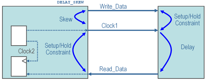
Timing Configuration for External Loop Clock
This is a system where a controller generates a read and write clock, and the read clock is looped back to the controller (see below).

In this system writes (Controller to Memory) are Source-Synchronous and reads (Memory to Controller) are synchronous. The controller will need a DELAY_SKEW statement for the Clock1 to Write_Data relationship as shown below:
DELAY_SKEW R Clock1_out *TO Write_Data SKEW_MIN SKEW_MAX
CLOCK_SKEW Clock1_out *TO Clock2_out SKEW_MIN SKEW_MAX
SETHLD Read_Data *TO R Clock2_in SETUP HOLD
The memory timing model would have a DELAY statement for the Clock1 to Read_Data timing relationship, as shown below:
DELAY R Clock1_in *TO Read_Data DELAY_MIN DELAY_MAX
SETHLD Write_Data *TO R Clock2_in SETUP HOLD
Timing Configuration for Internal Loop Clock
If the clock labeled Clock2 in the diagram above for "External Loop Clock" were inside the controller, the system would look like this:
The read and write timing is the same as in the external case (see User Guide section 13.4: "Pre-layout vs. Post-layout timing"), except the clock for the read data is internal to the controller. The data sheet timing references the Setup and Hold of the read data to Clock1, the output clock from the controller. Parallel Link Designer still requires an input clock for the Setup and Hold constraint for read data at the controller, so a dummy input clock must be created. This dummy input clock has a DELAY NX statement with zero delay to Clock1, so it has the same timing as Clock1. The configuration is shown below:
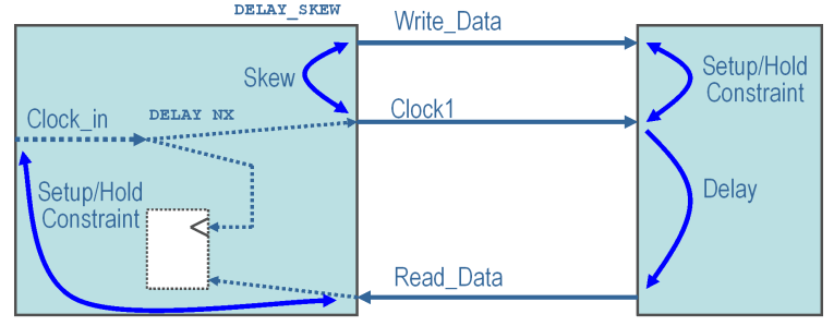
The dummy input clock pin can be an existing unused clock pin in the IBIS file, or a pin can be added to the IBIS component and timing model PINDEF. No Transfer Net is required for the dummy input clock. It is only used to create a common reference point for the synchronous timing calculation for data reads.
The controller timing model would have the following timing statements:
DELAY_SKEW R Clock1_out *TO Write_Data SKEW_MIN SKEW_MAX
DELAY NX Clock1_in *TO Clock1_out 0
SETHLD Read_Data *TO R Clock_in SETUP HOLD
The memory timing model would have a DELAY statement for the Clock1 to Read_Data timing relationship, as shown below:
DELAY R Clock1_in *TO Read_Data DELAY_MIN DELAY_MAX
SETHLD Write_Data *TO R Clock2_in SETUP HOLD
Summary
This tutorial has shown you how Parallel Link Designer can be used to analyze a Source-Synchronous-Clocked DDRx memory interface for Timing and Waveform Mask Analysis to determine compliance margins, as well as how some other clock architectures can be supported to analyze parallel-link systems.