Get Started with Parallel Link Designer
A parallel link interface is usually a bus with many data sources and/or destinations. You need to evaluate clock to data timing for each combination of driver and receiver on the parallel interface. It is also necessary to examine the shape of the waveform for each such combination. Problems such as inadequate amplitude, inadequate slew rate, or ringing can cause unreliable data transfer while problems such as overshoot can cause premature failure.
Each interface design must be evaluated both before and after the system and PC boards are designed. The pre-layout analysis is required if the design is to have any chance of working, and the post-layout analysis is required to make sure nothing was missed in the PC board design process. The net result is that there is usually a massive number of possibilities to analyze. These possibilities are the compounded combination of every combination of driver and receiver, every phase of the interface protocol, semiconductor process corners, PC board process corners separately for each layer of each PC board, passive component value, power supply voltages, temperature, and pre-layout and post-layout analysis. Failure to evaluate each and every one of these combinations increases the probability that problems will be identified much later in the design cycle, when correcting them is much more expensive.
The Parallel Link Designer app automates the running of the simulations by providing a graphical environment to set up the simulations and a standardized way in which to organize the model libraries. You can sift through the mass of data to identify information which is critical to the design in several ways:
A waveform analyzer evaluates output waveforms and identifies any waveforms which fail to meet predefined requirements.
A timing analyzer evaluates clock to data timing and identifies cases where the clock to data timing either fails to meet requirements or has minimal timing margin.
A separate spreadsheet is provided for waveform analyses and timing analyses. Each such spreadsheet organizes the data from summary information to the details of individual cases, thus making it practical to find detailed information about individual failing or marginal cases.
A waveform viewer makes it convenient to examine results graphically. Separate display panels are provided for waveforms and tabular results. Waveforms can be viewed in either the time domain or the frequency domain. Tabular results are presented in scatter plot format.
Organization of Simulations
To automate the simulation and analysis process, the Parallel Link Designer app organizes the work in a generic structure:
Project — A project is the top-level organization in the Parallel Link Designer app. All the work related to a particular product or system is usually contained in a project. A project can contain multiple interfaces.
Interface — Interface is the collection signals such as clock, data or strobe used to implement the physical layer protocol from the core one IC to the core of another IC. Example interfaces are: DDR, QDR, RLDRAM, PCIe, or XAUI.
Schematic Sheet — A schematic sheet is a graphical representation of the serial channel, captured using elements such as designators, transmission lines, s-parameters, vias and more. A schematic sheet is always a part of a schematic set.
Schematic Set — A schematic set is a collection of schematic sheets in an interface. Each schematic set may represent a different configuration of the Interface. In the Serial Link Designer app an interface can have one or more schematic sets.
The app also uses some specific terms to define certain elements that are useful:
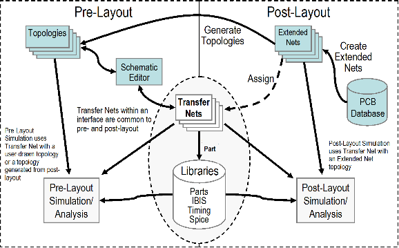
Transfer net — Each signal type in an interface is called a transfer net, and consists of the drivers, receivers, electrical conductors and passive components involved in transmitting that signal type. There may be multiple instances of a transfer net in an interface (example: data lines) or there could be a single instance (example: clock).
Transfer nets are common to both pre-layout analysis and post-layout verification. In pre-layout analysis, each sheet has an associated transfer net with the same name as the sheet. In post-layout verification, extended nets are assigned to transfer nets.
Solution space — Variations of parameters such as voltage, temperature, or process for each transfer net are organized into a solution space.
Designator — Within a transfer net, drivers and receivers are referred to as designators. In other words, a designator is either a starting point or an end point for a transfer net and is therefore a point where timing analysis is to be performed.
Pre-Layout and Post-Layout Analysis
In pre-layout analysis, each transfer net is described on a separate schematic sheet and is simulated in a separate simulation run. The circuit element values in a transfer net schematic can be parameterized so that many variations can be evaluated without having to change the schematic. Also, a transfer net schematic can contain crosstalk interferers, so that the analysis of the transfer net can be complete.

The purposes of pre-layout analysis are to:
evaluate multiple design options to identify proper I/O models, topology and termination,
identify crosstalk budgets and associated timing penalties,
and define layout rules for PCB design.
In post-layout analysis, each net on a PCB is called a CAD net. CAD nets can be combined with drivers, receivers, packages, discrete components and connector pins to form an extended net. An extended net contains designators and reaches from one IC to another. Extended nets can also traverse multiple PCBs. The Parallel Link Designer app provides convenient mechanisms for identifying extended nets and assigning them to transfer nets for all major PCB flows.
The purposes of post-layout analysis are to:
validate PCB routing,
validate PCB signal integrity and timing margins,
and validate crosstalk margins.
One of the advantages of the transfer net concept is that transfer nets can be re-used without modification from one phase of a project to another, or between projects. For example, if transfer nets were defined during the pre-layout phase of a project, then those definitions can be re-used without modification during the post-layout phase. Conversely, if a transfer net has been defined in the post-layout phase, it can be re-used directly in a pre-layout analysis
Libraries
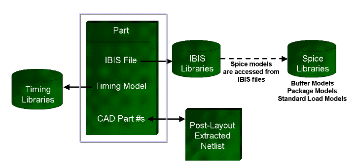
There are usually a number of different types of data associated with a given component, including electrical data such as HSPICE or IBIS models, timing models, and physical data such as CAD part number and pinout. For each component, all of this data is kept together in a Part, and every designator in a schematic must have a Part.

A Part has a unique identifier and contains references to an IBIS file, a timing model, and a CAD part number. An IBIS file, in turn, may contain:
mapping information between a part’s logical pin name, physical pin number, and I/O buffer model name,
behavioral I/O buffer models (for example, IV/VT curves),
references to HSPICE models and advanced package models,
and waveform processing levels which are MathWorks proprietary extensions to the IBIS standards.
The Parallel Link Designer app includes a 2D field solver which can be used to create accurate models of lossy transmission lines. There are well defined places to put libraries either for a single project or to be shared among many projects. The same library elements are used in pre-layout and post-layout analysis.
See Also
Parallel Link Designer | Signal Integrity Viewer