USB4 V2 Transmitter/Receiver IBIS-AMI Model
This example shows how to implement USB4 V2 (80Gbps PAM3) Transmitter and Receiver architectures with SerDes Designer and generate IBIS-AMI models using the library blocks in SerDes Toolbox™. The generated models conform to the IBIS-AMI and USB4 V2 specifications.
Transmitter and Receiver Setup in SerDes Designer App
The first part of this example sets up the target transmitter and receiver model architecture for Captive Device transmitter compliance testing. The second part of this example will demonstrate the construction of a reference receiver for a router assembly based on USB4 V2 eCOM (enhanced Channel Operating Margin). You will see how to create these data path blocks for USB4 V2 with the SerDes Designer app. In the third part of this example, you will export the system to Simulink® for further customization. The fourth part concludes this example with exporting IBIS-AMI models for use in any EDA tool capable of IBIS simulation such as Serial Link Designer from Signal Integrity Toolbox™.
Reference Files for SerDes Designer in MATLAB
This example uses the SerDes Designer models usb4p0v2_tx_comp.mat and usb4p0v2_rx_ref.mat as example systems you may reference. The first is to test Transmitter compliance (from USB4 V2 Specification, section 3.2.5.1) and the second is to implement a reference Receiver based on eCOM (see "USB 80G PHY background.pdf" in the reference section). Type the following command in the MATLAB® command window to open the first model with SerDes Designer:
>> serdesDesigner('usb4p0v2_tx_comp');
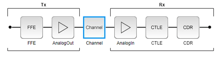
Part 1: System Configuration for Captive Device
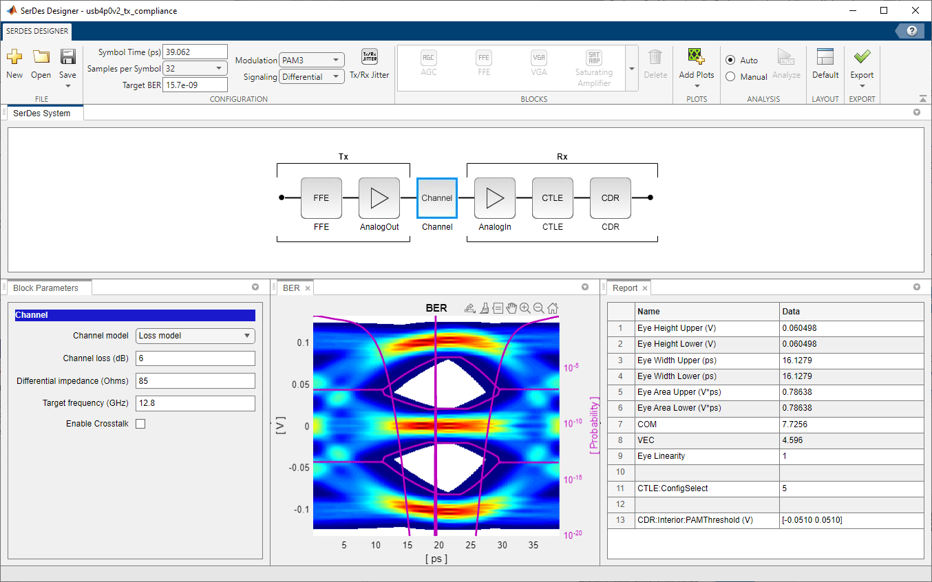
The SerDes Designer app will load a system representing USB4 V2 for Captive Device transmitter and receiver compliance. This includes a Transmitter having an FFE, a Captive Device Receiver with CTLE and CDR along with analog characteristics and an example channel as shown below.
You can see from the SerDes Designer app options that the following are already configured based on the USB4 V2 specification (USB4 Version 2.0, October 2022 edition):
Symbol Time is set to 39.0625ps (From 25.6 Giga-baud data rate given by Section 3.2.3, Table 3-22 and eCOM table)
Target BER is set to 15.7e-09
Note: Trit Error Ratio (TER) of 1e-08 is specified (Section 3.2.4.2) and you can find Bit Error Ratio as follows:
Samples per Symbol is set to 32 (Section 3.2.3, Table 3-23)
Modulation is set to PAM3 (Section 3.2.3, Figure 3-29)
Signaling is set to Differential (Section 3.2.3, Table 3-22)
Channel Model
You can click on the channel model block to observe the following configuration settings:
Channel loss is set to 6dB (This is an example, not a maximum loss channel- see Section 3.2.5.3, Figure 3-40).
Differential impedance is set to 85 Ohms (From 42.5 Ohms single-ended, Section 3.1.2.6, Compliance Boards).
Target Frequency is set to the Nyquist frequency of 12.8 GHz (From 25.6 Giga-baud data rate given by Section 3.2.3, Table 3-22 and eCOM table).
Transmitter Model: Configure AnalogOut Block
You click on the Tx AnalogOut block to observe the following configuration settings:
Voltage is 0.4 V (from eCOM spreadsheet value for "A_v" and TX Voltage Swing from USB 80G PHY Background PDF)
Rise time is 7.8125 ps (From Rt defined as 0.2*UI, Section 3.2.3, Table 3-22)
R (single-ended output resistance) is 42.5 Ohms (Section 3.1.2.6, Compliance Boards)
C (capacitance) is 0.1 pF (default value, not defined in specification).
Transmitter Model: Configure FFE Block
The Tx FFE block is set up for two pre-taps and one post-tap by including four tap weights, with presets as defined in the USB4 V2 specification, Table 3-24. This is done with the vector [0 0 1 0], where the main tap is specified by the largest value in the vector. You can click on the Tx FFE block to observe the following configuration settings:
FFE Tap is [0 -0.05 0.9 -0.05] (Section 3.2.3.8, Table 3-24, Preset Number 5)
Normalize Taps is Checked / Enabled (required per USB4 V2 specification, Table 3-24 notes)
Note: This is a tap selected manually to represent reasonable performance given the configuration of the channel block above.
Receiver Model for Captive Device: Configure AnalogIn Block
You can click on the Rx AnalogIn block to observe the following configuration settings:
R (single-ended input resistance) is 42.5 Ohms (Section 3.2.4.1, Table 3-26).
C (capacitance) is 0.2 pF (default value, not defined in specification).
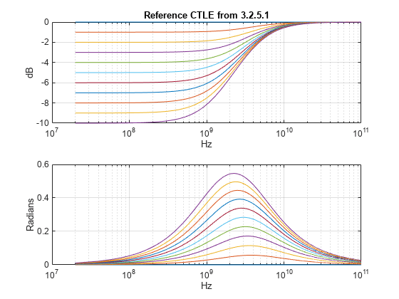
Receiver Model for Captive Device: Find CTLE Response
The Rx CTLE for TX compliance is defined according to the USB4 V2 specification, section 3.2.5.1:
Where:
is the DC Gain
The following code block shows how to find a GPZ matrix that represents the Rx CTLE used for Captive Device transmitter compliance. You will see how to visualize its response curve plots. After finding a GPZ matrix, the next step will be to add this configuration to the CTLE block that is part of the Receiver structure.
Note: The SerDes CTLE model requires that more poles be defined than zeros. In the code below, you will see we will pad an extra pole at high enough frequency to not disturb the signal but allow the model to have more poles than zeros and be stable.
%Reference RX CTLE for Captive Device transmitter measurements, USB4 V2 specification, section 3.2.5.1.
clear;
DCgain = 0:10;
ADC = 10.^(-DCgain/20);
p1 = 4e9; %Hz
wp1 = 2*pi*p1;
f = linspace(0,100e9,5001);
w = 2*pi*f;
s = 1j*w;
H = zeros(length(ADC),length(f));
for ii = 1:length(ADC)
    H(ii,:) = (s + ADC(ii)*wp1)./(s + wp1);
end
figure(1)
subplot(211);
semilogx(f,db(H))
grid on
xlabel('Hz')
ylabel('dB')
title('Reference CTLE from 3.2.5.1')
subplot(212);
semilogx(f,unwrap(angle(H)))
grid on
xlabel('Hz')
ylabel('Radians')
ppad = 200e9;

gpz = zeros(length(ADC),4);
gpz(:,1) = -DCgain;
gpz(:,2) = -p1;
gpz(:,3) = -p1*ADC;
gpz(:,4) = -ppad;
Receiver Model for Captive Device: Configure CTLE Block
In the Rx CTLE block, you can set the Specification to GPZ Matrix and insert the workspace variable gpz into the Gain pole zero matrix dialog box (Note: you can use the workspace variable name, or the contents of that variable in this dialog box). Then set the CTLE Mode to adapt. The Rx CTLE block is set up for 11 configurations (representing Gains of 0 to -10dB in steps of -1dB). The GPZ (Gain Pole Zero) matrix data is derived from the transfer function of the behavioral CTLE (USB4 V2 specification, section 3.2.5).
Receiver Model for Captive Device: Configure CDR Block
You can see a CDR block has been placed within the Receiver structure, this will enable clock-domain recovery to be configured at a later time.
Receiver Model for Captive Device: Plot Statistical-Mode Results
Note that a minimum compliance for the Receiver (which may be used to evaluate Eye Diagrams) is defined by the USB4 V2 specification (Section 3.2.6.2, Table 3-31 and Figure 3-42) as follows:
Voltage Margin Range, Minimum: +/- 74/2 mV or 37mVpp
Voltage Margin Range, Maximum: +/- 200/2 mV or 100mVpp
Timing Margin Range, Minimum: +/- 0.2 UI
Timing Margin Range, Maximum: +/- 0.5 UI
Jitter Parameters for Transmitter
You can add Jitter parameters based on the eCOM table for the USB4 V2 by selecting the Tx/Rx Jitter button and setting the values as follows:
Note: These parameters will export as type "Float" with format "Value." After exporting to Simulink, you can change these to format "Range" using the IBIS-AMI Manager, to set 0 UI as default value for simulation.
Tx Rj Jitter Value
Set value to
0.0085(Note: this is the maximum allowed per eCOM table v1.1, where0UI is nominal).Set units to UI.
Enable Tx_Rj by checking the box and observe in real time how the eye diagram and report values change.
Tx Sj Jitter Value
Set value to
0.024704(Note: this is the maximum allowed per eCOM table v1.1, where0UI is nominal).Set units to UI.
Enable Tx_Sj.
Jitter Parameters for Receiver
Rx Rj Jitter Value
Set value to
0.013124405(Note: this is the maximum allowed per eCOM table v1.1, where0UI is nominal).Set units to UI.
Enable Rx_Rj.

You can use the SerDes Designer plots to visualize the performance of the USB4 V2 system in Statistical Mode. You can then select the options BER and Report from Add Plots drop down in the toolstrip and observe the results to compare performance against the Voltage and Timing margin ranges given above.
Note: You can also add a plot to visualize the CTLE Transfer Function.
You may observe that the Statistical Eye and BER plot appear to be more closed with jitter parameters enabled, but this is expected. The jitter parameters from the specification are maximum allowed values and there is no expectation they would each be maximum at the same time in a real-world system. The reason you are enabling these jitter parameters is so they are automatically included in this SerDes System when exporting to Simulink. Later you will see how to change these to format "Range" in the IBIS-AMI manager and set each one to 0 UI as a default value.
Note: After exporting to Simulink, you can also edit their Type, Usage, Format, and Value using the IBIS-AMI manager.
Part 2: System Configuration for Router Assembly with Reference Receiver
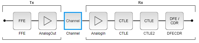
The SerDes Designer app will load a system representing a router assembly described by the USB4 V2 specification: The Transmitter is retained from the Captive Device topology discussed in the first part of this example and shows a Reference Receiver for a Router Assembly based on the eCOM table for USB4 V2 (see reference section). This includes a Transmitter having an FFE, a Router Assembly Receiver with CTLE and DFECDR along with analog characteristics and an example channel as shown below.
Use the MATLAB® command window to open the second model usb4p0v2_rx_ref.mat with SerDes Designer:
>> serdesDesigner('usb4p0v2_rx_ref');
You can see from the SerDes Designer app options that the following remain configured the same as Part 1 above:
Symbol Time: 39.0625ps
Target BER: 15.7e-09
Samples per Symbol: 32
Modulation: PAM3
Signaling: Differential
Channel Model
This also retains the configuration from Part 1 above:
Channel loss: 6dB
Differential impedance: 85 Ohms
Target Frequency: 12.8 GHz
Transmitter Model: AnalogOut Block
In the transmitter section, the Tx AnalogOut block remains the same from Part 1 above:
Voltage: 0.4 V
Rise time: 7.8125 ps
R: 42.5 Ohms
C: 0.1 pF (default value, not defined in specification).
Transmitter Model: Configure FFE Block
The Tx FFE remains the same as Part 1 above:
FFE Tap is [0 -0.05 0.9 -0.05] (Preset 5)
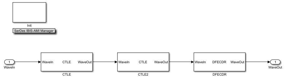
Receiver Model for Router Assembly: Summary
Note that the CTLE block portion of the Receiver model differs from Part 1 above, in that there are 2 stages represented by 2 blocks, and there is the addition of a DFECDR block as well.
Receiver Model for Router Assembly: Configure AnalogIn Block
You can click on the Rx AnalogIn block to observe the following configuration settings, which are identical to Part 1 above:
R: 42.5 Ohms
C: 0.2 pF (default value, not defined in specification).
Receiver Model for Router Assembly: Find CTLE Response based on eCOM
Note that from this point forward, the Receiver model differs from Part 1 above, in that a reference eCOM receiver is described as having a 2-stage CTLE with 12-tap DFE and CDR (see "eCOM_general_config_rev1p1.xlsx" reference below). The Rx CTLE is defined as having 2 stages with the following transfer equation (see "USB 80G PHY Analysis v1p1.pptx" reference below):
Where:
: DC Gain for CTLE stage 1 ("high pole" stage): 0 to -12dB in steps of 1dB
: Pole location for CTLE stage 1: 10.24GHz
: Zero location for CTLE stage 1: 10.24GHz
: 2nd Pole location for CTLE stage 1: 25.6GHz
: DC Gain for CTLE stage 2 ("low pole" stage): 0 to -6dB in steps of 1dB
: Pole location for CTLE stage 2: 0.32GHz
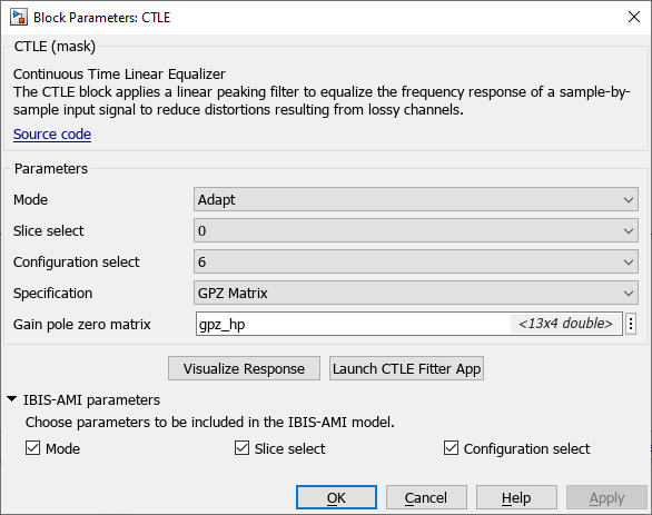
The following code block shows how to find a GPZ matrix that represents the Rx CTLE stage 1 ("high pole"). You can then add this GPZ matrix (as you were shown in Part 1 above) to the first CTLE block (named CTLE) in the Receiver structure.
% CTLE Stage1 (high pole) given by eCOM reference table for USB4 V2.
DCgain_hp = 0:12;
ADC_hp = 10.^(-DCgain_hp/20);
hp_z1 = 10.24e9; %Hz
hp_wz1 = 2*pi*hp_z1;
hp_p1 = 10.24e9; %Hz
hp_wp1 = 2*pi*hp_p1;
hp_p2 = 25.6e9; %Hz
hp_wp2 = 2*pi*hp_p2;

f = linspace(0,100e9,5001);
w = 2*pi*f;
s = 1j*w;

H = zeros(length(ADC_hp),length(f));
for ii = 1:length(ADC_hp)
    H(ii,:) = (hp_p1*(s+hp_wz1*ADC_hp(ii)))./(hp_z1*(s+hp_wz1)).*((hp_wp2)./(s+hp_wp2));
end

figure(10)
subplot(211);
semilogx(f,db(H))
grid on
xlabel('Hz')
ylabel('dB')
title('CTLE Stage1 (high pole) given by eCOM reference table from USB4 V2.')
subplot(212);
semilogx(f,unwrap(angle(H)))
grid on
xlabel('Hz')
ylabel('Radians')
% Create a GPZ matrix for use in a CTLE block:
gpz_hp = zeros(length(ADC_hp),4);
gpz_hp(:,1) = -DCgain_hp;
gpz_hp(:,2) = -hp_p1;
gpz_hp(:,3) = -hp_z1*ADC_hp; %z1
gpz_hp(:,4) = -hp_p2;
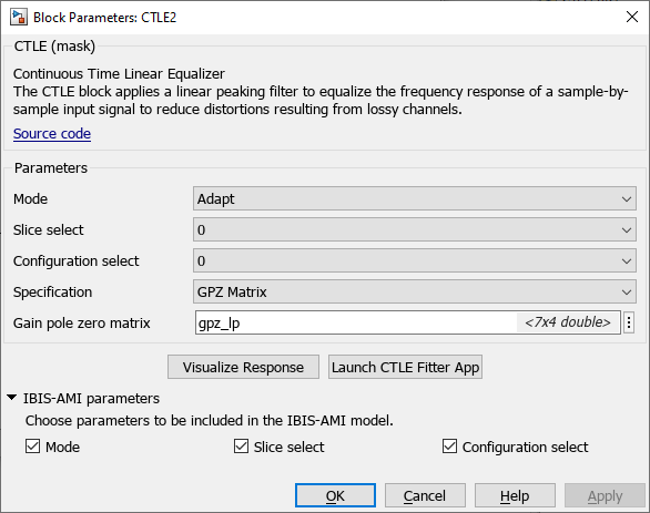
The following code block shows how to find a GPZ matrix that represents the Rx CTLE stage 2 ("low pole"). You can then add this GPZ matrix (as you were shown in Part 1 above) to the second CTLE block (named CTLE2) in the Receiver structure (where there are two CTLE blocks: one CTLE block per stage).
%CTLE Stage2 (low pole) given by eCOM reference table for USB4 V2.
DCgain_lp = 0:6;
ADC_lp = 10.^(-DCgain_lp/20);
lp = 0.32e9; %Hz
wlp = 2*pi*lp;

f = linspace(0,100e9,5001);
w = 2*pi*f;
s = 1j*w;

H = zeros(length(ADC_lp),length(f));
for ii = 1:length(ADC_lp)
    H(ii,:) = (s + wlp*ADC_lp(ii))./(s + wlp);
end

figure(3)
subplot(211);
semilogx(f,db(H))
grid on
xlabel('Hz')
ylabel('dB')
title('CTLE Stage2 (low pole) given by eCOM reference table from USB4 V2.')
subplot(212);
semilogx(f,unwrap(angle(H)))
grid on
xlabel('Hz')
ylabel('Radians')

ppad = 200e9;

gpz_lp = zeros(length(ADC_lp),4);
gpz_lp(:,1) = -DCgain_lp;
gpz_lp(:,2) = -lp;
gpz_lp(:,3) = -lp*ADC_lp;
gpz_lp(:,4) = -ppad;
Receiver Model for Router Assembly: Define DFE Taps
The Rx DFECDR block is defined according to the eCOM table from USB4 V2 as having the following characteristics:
Tap Count: 12
Range of Tap 1: 0 to +0.75
Range of Taps 2 through 12: -0.2 to +0.2
Part 3: Export SerDes System to Simulink
Click on the Export button to export the second of the above configurations to Simulink for further customization and generation of the AMI model executables. This configuration contains both the Transmitter and reference Receiver models.
Review Simulink Model Configuration
The SerDes System imported into Simulink consists of the Configuration, Stimulus, Tx, Analog Channel and Rx blocks. All the settings from the SerDes Designer app have been transferred to the Simulink model. Save the model and review each block setup.
You can explore the configuration of the SerDes system in Simulink as follows:
Double click the Configuration block to open the Block Parameters dialog box. The parameter values for Symbol time, Samples per symbol, Target BER, Modulation and Signaling are carried over from the SerDes Designer app.
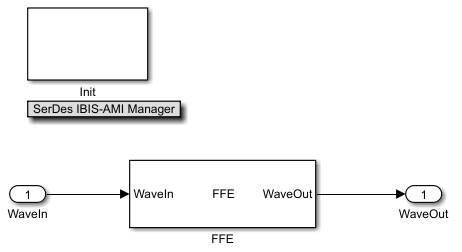
Double click the Tx block to look inside the Tx subsystem. The subsystem has the FFE block carried over from the SerDes Designer app. An Init block is also introduced to model the statistical portion of the AMI model.
Double click the Analog Channel block to open the Block Parameters dialog box. The parameter values for Target frequency, Loss, Impedance and Tx/Rx Analog Model parameters are carried over from the SerDes Designer app.
Double click on the Rx block to look inside the Rx subsystem. The subsystem has 2 CTLEs and 1 DFECDR block carried over from the SerDes Designer app. An Init block is also introduced to model the Statistical(Init) portion of the AMI model.
Double click the Stimulus block to open its Block Parameters dialog box. You will see how to configure this in the next step below.
Configure Stimulus Pattern
Open the Stimulus block and select the appropriate stimulus pattern for your system. For USB4 V2, set the Number of symbols to 50000, the Waveform creation method to Serial PRBS and then Binary to PAMn mapping to USB4V2.
Note: This configuration is based on section 4.3.2.2.1 of the USB4 V2 specification.
Update Transmitter AMI Parameters
Open the AMI-Tx tab in the SerDes IBIS/AMI manager dialog box. Following the format of a typical AMI file, the reserved parameters are listed first followed by the model specific parameters.
Simulink supports more sophisticated AMI model development compared to Serdes Designer, so you can create a selector for the Tx FFE to allow selection of the values from the presets specified in the USB4 V2 specification (Section 3.2.3, Table 3-24).
Setup Tx FFE
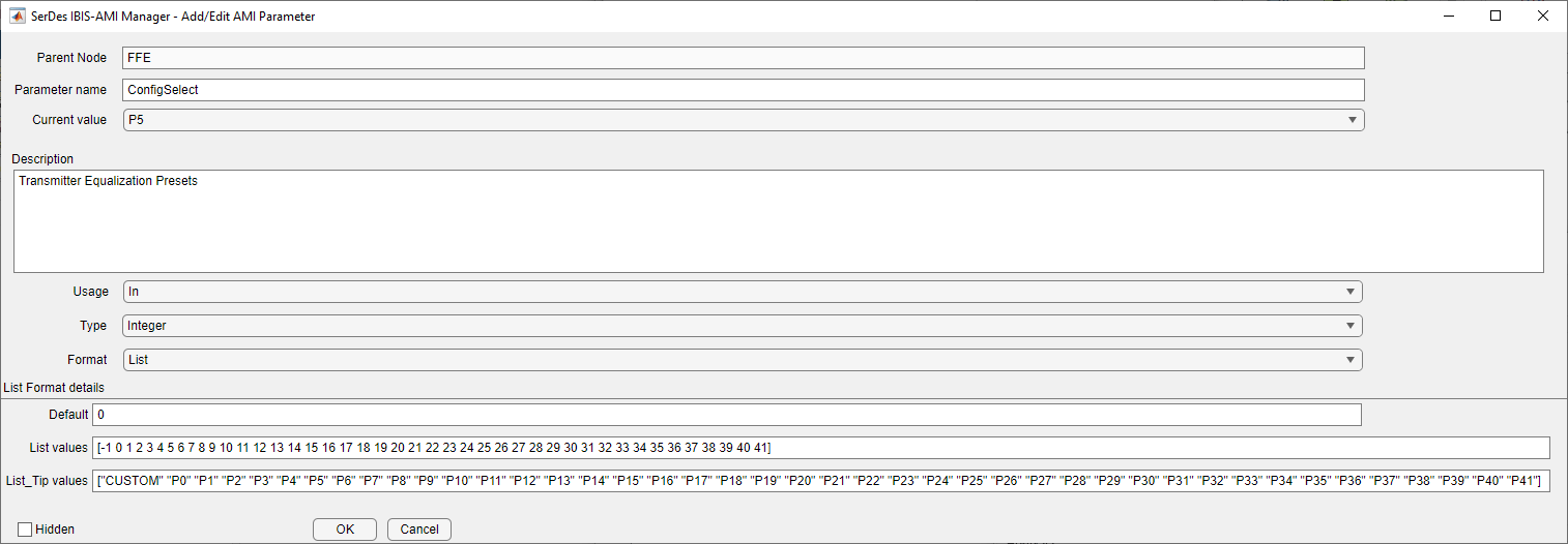
In the AMI - TX tab, under the Model_Specific parameters, you can click on FFE and then Add Parameter button to create a new AMI parameter "ConfigSelect."
Then select the new parameter ConfigSelect and click the edit button. In the next dialog box window, set the following values that represent Tx FFE Presets P0 through P41 (as defined by the PCIe Gen5 Base Specification).
Settings for the Add/Edit AMI Parameter ConfigSelect:
Parent Node FFE
Parameter name ConfigSelect
Current value P5
Description Transmitter Equalization Presets
Usage In
Type Integer
Format List
Default 0
List values [-1 0 1 2 3 4 5 6 7 8 9 10 11 12 13 14 15 16 17 18 19 20 21 22 23 24 25 26 27 28 29 30 31 32 33 34 35 36 37 38 39 40 41]
List_Tip values ["CUSTOM" "P0" "P1" "P2" "P3" "P4" "P5" "P6" "P7" "P8" "P9" "P10" "P11" "P12" "P13" "P14" "P15" "P16" "P17" "P18" "P19" "P20" "P21" "P22" "P23" "P24" "P25" "P26" "P27" "P28" "P29" "P30" "P31" "P32" "P33" "P34" "P35" "P36" "P37" "P38" "P39" "P40" "P41"]
Hidden = False (unchecked)
Tx FFE: Enable Tap-Preset Selector for Statistical (Init) Analysis
Modify the Initialize MATLAB function inside the Init block in the Tx subsystem to use the newly added ConfigSelect parameter. The ConfigSelect parameter controls the existing three transmitter taps. To accomplish this, add a switch statement that takes in the values of ConfigSelect and automatically sets the values for all three Tx taps, ignoring the user defined values for each tap. If a ConfigSelect value of -1 is used, then the user-defined Tx tap values are passed through to the FFE datapath block unchanged.
Look inside the Tx subsystem and you will see an FFE block along with a block called "Init."
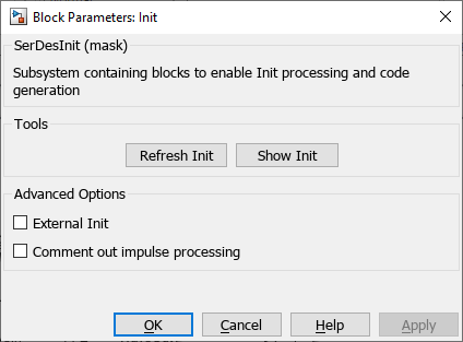
To edit the code that executes during statistical AMI simulation, double-click the Init block to open the Block Parameters dialog box and click the Refresh Init button to propagate the new AMI parameter to the Initialize sub-system.
Then click on Show Init to display the code in an editor window.
You will see the section for the Custom user code area shown thusly:
%% BEGIN: Custom user code area (retained when 'Refresh Init' button is pressed)
FFEParameter.ConfigSelect; % User added AMI parameter from SerDes IBIS-AMI Manager

% END: Custom user code area (retained when 'Refresh Init' button is pressed)
Add code for your Tx FFE Tap selector between the %% Begin and % End portions of Custom user code area. Or, you can copy the example code from the file Tx_FFE_Presets_Init.m attached to this example. This will allow for case/select for different Tx FFE Tap Preset values already configured in the IBIS-AMI manager.
Tx FFE: Enable Tap-Preset Selector for Time Domain (GetWave) Analysis
Enable Tx FFE tap presets in GetWave analysis with a new MATLAB function that operates in the same manner as the Initialize function. Inside the Tx subsystem, type Ctrl-U to look under the mask of the FFE block.
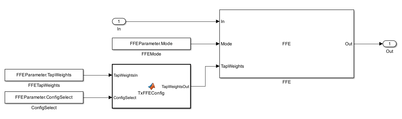
You can see that a new constant block has been added called FFEParameter.ConfigSelect. This is created automatically by the IBIS-AMI Manager when a new Reserved Parameter is added. Next, you can follow these steps to re-configure the selection of tap weight presets for time domain (GetWave) simulation:
Add a MATLAB Function block to the canvas from the Simulink/User-Defined library.
Rename the MATLAB Function block to Tx
FFEConfig.Double-click the MATLAB Function block and observe the template code now contains a function allowing case/select.
function TapWeightsOut = TxFFEConfig(TapWeightsIn, ConfigSelect)

switch ConfigSelect

    case 0

    otherwise

end
You can manually create the case/select values, or you can copy from the example code provided in the file Tx
FFEConfig.mattached to this example.Finally, wire up the Data Stores and new MATLAB function block as shown in the figure above.
Update Receiver AMI Parameters
Configure Rx CTLE Blocks
You can configure the CTLE blocks to contain the appropriate GPZ matrices. Each block should have one GPZ matrix. Due to the principle of Super Position, you can use either one. For the first CTLE block (CTLE), configure the following settings:
Mode: Adapt
Slice select: (0, default)
Configuration select: (any)
Specification: GPZ Matrix
GPZ Matrix: gpz_hp (Note: this references the MATLAB workspace variable created with the script above)
Then for the second CTLE block (CTLE2), configure the following settings:
Mode: Adapt
Slice select: (0, default)
Configuration select: (any)
Specification: GPZ Matrix
GPZ Matrix: gpz_lp (Note: this references the MATLAB workspace variable created with the script above)
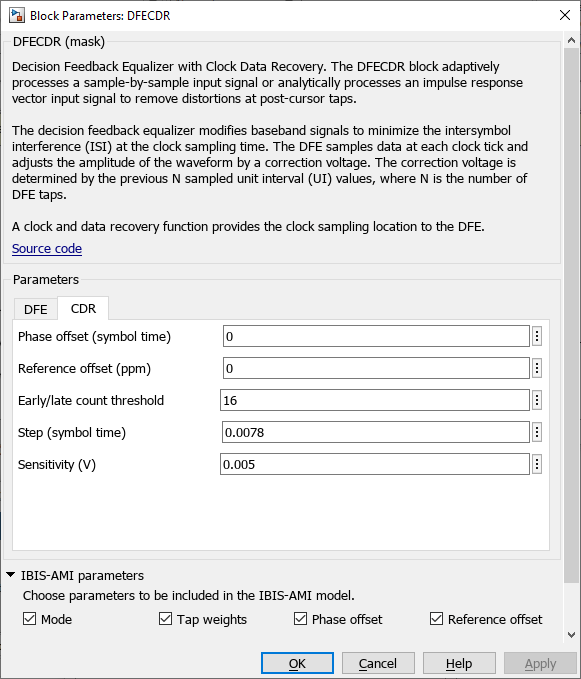
Configure Rx DFECDR Block
Simulink supports Time Domain simulation, so you can configure the DFECDR block to perform clock recovery based on UI and other parameters depending on your particular implementation. You will see how to configure the DFE portion and CDR sections of this block below:
Configure values in the DFE tab as follows:
Mode: Adapt
Initial tap weights (V): [0 0 0 0 0 0 0 0 0 0 0 0]
Adaptive gain: 9.6e-05
Adaptive step size (V): 1e-06
Minimum DFE tap values (V): [0 -0.2 -0.2 -0.2 -0.2 -0.2 -0.2 -0.2 -0.2 -0.2 -0.2 -0.2]
Maximum DFE tap values (V): [0.75 0.2 0.2 0.2 0.2 0.2 0.2 0.2 0.2 0.2 0.2 0.2]
2x Tap Weights = False (unchecked):
IBIS-AMI Parameters:
Mode: Enabled
Tap weights: Enabled
Phase offset: Enabled
Reference offset: Enabled
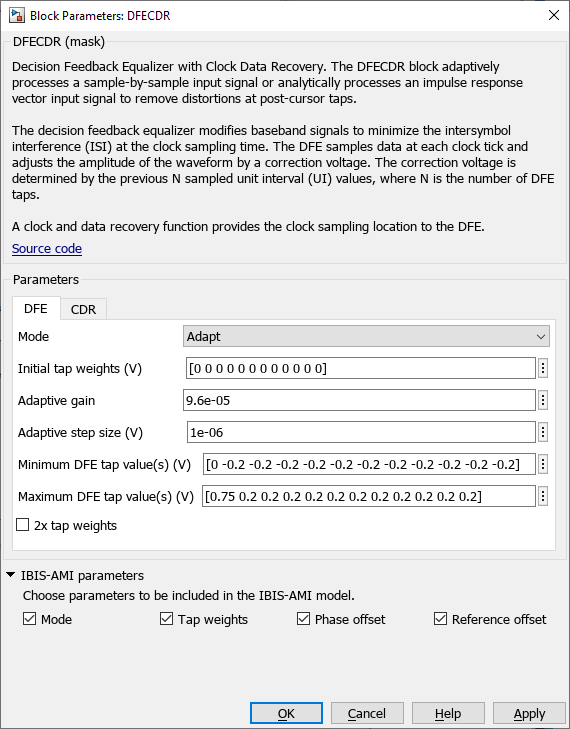
Next, click on the CDR tab. Assuming that the CDR transfer function and the jitter transfer function are compliments to each other and that they touch at the 3dB point, we can infer that the CDR bandwidth needs to be 6 MHz (Section 3.2.2.2, USB4 V2 Specification).
The following is an approximate way of determining the bandwidth of the digital SerDes CDR (see Count under serdes.CDR in the MATLAB documentation).
or
So given the Bandwidth and Symbol time of the link, we could adjust the count and step parameters to provide a reasonable response. With this in mind, configure values in the CDR tab as follows:
Phase offset is set to 0 UI (symbol time)
Reference offset is set to 0 ppm
Early/late count threshold is set to 16 (default)
Step is set to 0.00244 (symbol time)
Sensitivity is set to 0.005 V (For purposes of this example, this is set to match the note "slc_det_noise" from the eCOM spreadsheet (also matching the Slicer Sensitivity given in the USB 80G PHY Background PDF). Otherwise, you may set it to approximately 10% of a valid eye height- you may adjust this to represent the actual value for receiver sensitivity in your system design)
Configure Run-Time Parameters with IBIS-AMI Manager
Open the Block Parameter dialog box for the Configuration block and click on the SerDes IBIS-AMI Manager button. In the IBIS tab inside the SerDes IBIS-AMI manager dialog box, the analog model values are converted to standard IBIS parameters that can be used by any industry standard simulator. They also contain run-time parameters that would be used by those EDA tools, and are also used by Simulink for this simulation.
Note: Confirm that each Jitter parameter default values are set to 0 for both the Transmitter and Receiver in the SerDes IBIS-AMI Manager.
Click on the Export tab and set the following:
AMI Model Settings – Tx:
Bits to ignore: 4
AMI Model Settings – Rx:
Bits to ignore: 30000 (Note: IBIS-AMI Ignore Bits must be fewer than the symbol count set in Stimulus block in order to display Time Domain Waveforms)
Test the USB4 V2 System with Simulink
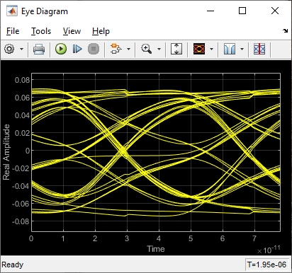
You can click on the Run button in the Simulink toolstrip simulate the SerDes System representing USB4 V2. Two plots are generated. The first is a time domain (GetWave) eye diagram that is updated as the model is running.
Note: This may appear differently in your Simulink session depending on your specific viewer settings or SerDes system configuration.
A second plot is presented after simulation has completed which contains views of the Statistical (Init) and Time Domain (GetWave) results:
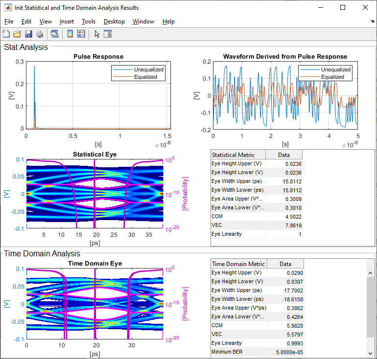
Note: You may observe a difference between Statistical and Time Domain waveforms. In Time Domain simulation, the effects of symbol encoding (e.g. to control ISI) and also real time DFE (Decision Feedback Equalizer) behavior may contribute to improved performance. Conversely, Statistical simulation utilizes frequency-domain Convolution rather than symbol-by-symbol stimulus, and does not include the effects of symbol encoding or signal conditioning by a DFE. Further discussion is beyond the scope of this example, but you may consider other differences between the simulation types as well by researching Communications Theory and the IBIS specification reference provided below.
Part 4: Generate and Export IBIS-AMI Models
The fourth part of this example takes the customized Simulink model, modifies the AMI parameters for USB4 V2, then generates IBIS-AMI compliant model executables, IBIS and AMI files.
Open the Block Parameter dialog box for the Configuration block and click on the SerDes IBIS-AMI Manager button. In the IBIS tab inside the SerDes IBIS-AMI manager dialog box, the analog model values are converted to standard IBIS parameters that can be used by any industry standard simulator. In the AMI-Tx and AMI-Rx tabs in the SerDes IBIS-AMI manager dialog box, the reserved parameters are listed first followed by the model specific parameters following the format of a typical AMI file.
Export IBIS-AMI Models
Select the Export tab in the SerDes IBIS-AMI manager dialog box.
Update the Tx model name to usb4p0v2_tx.
Update the Rx model name to usb4p0v2_rx.
Note that the Tx and Rx corner percentage is set to 10%. This will scale the min/max analog model corner values by +/-10%.
Verify that Dual model is selected for both the Tx and the Rx. This will create model executables that support both statistical (Init) and time domain (GetWave) analysis.
Set the Tx model Bits to ignore value to 4 since there are three taps in the Tx FFE.
Set the Rx model Bits to ignore value to 30000 to allow sufficient time for the Rx DFE taps to settle during time domain simulations.
Verify that Both Tx and Rx are set to Export and that all files have been selected to be generated (IBIS file, AMI files, .dll files [Windows] and/or .so files [Unix/Linux]).
Set the IBIS file name to be usb4p0v2.ibs.
You can now observe the IBIS-AMI manager looks as follows, where your system is ready to export IBIS-AMI models:
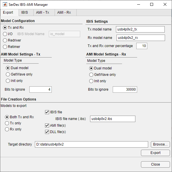
Press the Export button to generate models in the Target directory.
Test Generated IBIS-AMI Models
The USB4V2 transmitter and receiver IBIS-AMI models are now complete and ready to be utilized within any industry EDA tool capable of IBIS-AMI simulation, such as Serial Link Designer from Signal Integrity Toolbox.
References
[1] USB-IF USB4 V2 Specification, October 2022 Edition, https://usb.org/.
[2] USB4 V2 Artifact, "USB 80G PHY background.pdf", https://usb.org/.
[3] USB4 V2 Artifact, "eCOM_general_config_rev1p1.xlsx", https://usb.org/.
[4] IBIS 7.1 Specification, https://ibis.org/ver7.1/ver7_1.pdf.
[5] Channel Operating Margin (COM) (Signal Integrity Toolbox)
See Also
SerDes Designer | FFE | CTLE | CDR