Generate HSPICE Simulation Decks for IBIS Characterization
R2026bYou can write your own HSPICE or Spectre simulation decks (testbenches) to produce the input data for the IBIS Designer SPICE Simulation workflow. Before you create an IBIS model from simulation data, you must run three types of SPICE simulations against your transistor-level buffer model: IV (DC sweep), VT (transient), and AC (admittance). This topic provides annotated deck templates for every combination of model type (Input, Output, I/O) and signaling mode (single-ended, differential).
Note: These decks are written for Synopsys HSPICE. To use them with Cadence Spectre, the behavioral model elements (VCR, PWL sources) and the analysis and output statements require rewriting. The testbench topology and characterization methodology are simulator-independent.
When to use this workflow:
You have a transistor-level SPICE model of your I/O buffer and want to produce characterization data for IBIS Designer.
You are setting up an IBIS extraction flow for the first time and want to understand the testbench requirements.
You want to compare single-ended and differential testbench approaches.
Overview: Three Simulation Types
You need data from three simulation types to construct a complete IBIS model. Each type captures a different aspect of the buffer's electrical behavior:
Simulation | HSPICE Analysis | What It Captures | IBIS Data Generated |
|---|---|---|---|
IV |
| Static current vs. voltage at the pad | Pulldown IV, Pullup IV, GND Clamp, POWER Clamp |
VT |
| Dynamic voltage vs. time into a fixture | Rising/Falling waveforms at GND and VDD fixtures |
AC |
| Small-signal capacitance at the pad | C_comp (die capacitance) |
To produce the typ/min/max data in the IBIS file, run each simulation type at three process corners (typical, slow, fast). The decks shown here are for the typical corner. See "Corner Variation" for what to change for slow and fast corners.
Workflow: From SPICE Model to Simulation Data
Follow these seven steps to generate a complete set of characterization data. The sections below provide detail and templates for each step.
Prepare your buffer subcircuit. Verify that your transistor-level SPICE model simulates correctly in HSPICE. Identify its port interface.
Create wrapper subcircuits. Write a thin wrapper (
.subckt) that maps your model's native port names to the standard port order that the characterization decks expect (see "Subcircuit Port Interface Convention" below).Choose deck templates. Choose the appropriate templates for your model type (Input, Output, I/O) and signaling mode (single-ended or differential). See "Required Decks per Model Type" for the full matrix.
Point decks at your wrapper. Edit the
.includeand.subcktcalls in each template to reference your wrapper file and subcircuit name.Create corner variants. Duplicate each typical-corner deck for slow and fast corners. Modify temperature, supply voltage, driver resistance, and model card parameters as described in "Corner Variation."
Name output files. Configure HSPICE output filenames to follow the
{type}_{corner}_{modelname}.{ext}convention so IBIS Designer auto-fill can locate them (see "File Naming Convention").Run simulations. Execute all decks (3 corners x 3-4 simulation types). Verify convergence and check that output waveforms look physically reasonable before you import into IBIS Designer.
Subcircuit Port Interface Convention
All decks use a .include directive to reference your SPICE subcircuit model. Your subcircuit must follow a specific port order that depends on the model type:
Single-Ended Models:
Model Type | Port Order | Notes |
|---|---|---|
Input |
| No driver ports |
Output |
| No enable or receiver ports |
I/O |
| Full interface |
Differential Models:
Model Type | Port Order | Notes |
|---|---|---|
Input |
| Complementary pad added |
Output |
| Complementary pad added |
I/O |
| Full interface |
Port definitions:
vddq / vssq: Power supply and ground for the I/O domain
pad / pad_n: Buffer output pad (and complement for differential)
vstim: Digital stimulus input controlling the driver state (0 = pull low, 1 = pull high)
enable: Output enable (1 = driver active, 0 = high-impedance/receiver mode)
corein: Core-side receiver output (terminated through a high-impedance load)
IV Deck: DC Sweep for Current-Voltage Curves
The IV simulation sweeps the pad voltage across the full operating range and measures the current into the buffer at each voltage point. This sweep produces the four IV curves that define the buffer's static behavior in IBIS:
Pulldown IV: Current when the driver is pulling the pad toward ground (stimulus=0, enable=1)
Pullup IV: Current when the driver is pulling the pad toward Vdd (stimulus=1, enable=1)
GND Clamp IV: Current through the ESD/termination path below ground (enable=0)
POWER Clamp IV: Current through the ESD/termination path above Vdd (enable=0)
Key IV Deck Elements
Sweep source with isolation resistor:
You sweep the pad voltage with a voltage source (Vv_sweep_r) through a small isolation resistor (0.1 ohm). This resistor prevents numerical convergence issues when the sweep source drives a low-impedance node directly:
Vv_sweep_r v_sweep_r 0 DC 0.
.DC Vv_sweep_r '-Vdd' '2*Vdd' 0.010
Rol v_sweep v_sweep_r 0.1
Sweep range: You sweep the voltage from -Vdd to 2*Vdd. This range captures both clamp regions (below GND and above Vdd) and the full driver operating range.
Voltage-sensing ammeter (V-source at 0V): A zero-volt voltage source in series with the pad measures the current. The .probe dc i(Vol) statement records this current. Here Vol is the name of the voltage source (not a voltage level); i(Vol) is the current through that source:
Vol v_sweep pad_L DC 0.
.probe dc i(Vol)
Single-Ended I/O: IV Deck Structure
The I/O model requires three DUT instances in the same deck, one for each operating condition. The third instance (clamp/receiver mode) captures the passive current path that is present in receiver mode. You must subtract this current from the pullup and pulldown measurements to isolate the pure driver contribution.
The reference deck spice_decks/iv_se_io.spi implements this structure:
unzip spice_decks.zip;
disp(fileread(fullfile(pwd, "spice_decks", "iv_se_io.spi")))
* IBIS Characterization: IV (DC Sweep) - Single-Ended I/O
*
* This deck sweeps the pad voltage from -Vdd to 2*Vdd and measures:
*   - Pulldown current (Vol): driver enabled, stimulus=0
*   - Pullup current (Voh):   driver enabled, stimulus=1
*   - Clamp/ODT current (Vor): driver disabled (receiver mode)
*
* Post-processing with CCVS (H) and VCCS (G) elements isolates the raw
* pullup and pulldown currents by subtracting the clamp contribution.
*
* Your subcircuit must have this port order:
*   .subckt <name> vddq vssq pad vstim enable corein
*
* Required parameters on the subcircuit instance line:
*   rout   - driver output resistance (ohms)
*   odt   - on-die termination resistance (ohms)
*   cpad  - die capacitance at pad, for IBIS C_comp (F)
*   rdie  - internal die RC series resistance (ohms)
*   cdie  - internal die RC capacitance (F)
*

.include 'your_model.sp'

*--- Simulation Setup --------------------------------------------------------
.temp 25
.options post probe
.DC Vv_sweep_r -1.1 2.2 0.010

*--- Sweep Source (with 0.1-ohm isolation resistor) --------------------------
Vv_sweep_r v_sweep_r 0 DC 0.
Rol v_sweep v_sweep_r 0.1
.probe dc v(v_sweep)

*--- Supply ------------------------------------------------------------------
.param vdd = 1.1

*=============================================================================
* Pulldown Instance (_L): enable=1, stimulus=0
*=============================================================================
Vlow stim_L 0 DC 0.
Vol  v_sweep pad_L DC 0.
.probe dc i(Vol)

Vvddq_L vddq_L 0 DC 'vdd'
Vvssq_L vssq_L 0 DC 0.
Ven_L   en_L   0 DC 1.
Rcore_L core_L 0 1Meg

Xbuf_L vddq_L vssq_L pad_L stim_L en_L core_L
+ your_model rout=34 odt=50 cpad=0.9pF rdie=1e-3 cdie=1e-18

*=============================================================================
* Pullup Instance (_H): enable=1, stimulus=1
*=============================================================================
Vhigh stim_H 0 DC 1.
Voh   v_sweep pad_H DC 0.
.probe dc i(Voh)

Vvddq_H vddq_H 0 DC 'vdd'
Vvssq_H vssq_H 0 DC 0.
Ven_H   en_H   0 DC 1.
Rcore_H core_H 0 1Meg

Xbuf_H vddq_H vssq_H pad_H stim_H en_H core_H
+ your_model rout=34 odt=50 cpad=0.9pF rdie=1e-3 cdie=1e-18

*=============================================================================
* Clamp Instance (receiver mode): enable=0
* Measures the passive current path (ESD clamps + ODT) that is always present
*=============================================================================
Voff stim_R 0 DC 0.
Vor  v_sweep pad_R DC 0.
.probe dc i(Vor)

Vvddq_R vddq_R 0 DC 'vdd'
Vvssq_R vssq_R 0 DC 0.
Ven_R   en_R   0 DC 0.
Rcore_R core_R 0 1Meg

Xbuf_R vddq_R vssq_R pad_R stim_R en_R core_R
+ your_model rout=34 odt=50 cpad=0.9pF rdie=1e-3 cdie=1e-18

*=============================================================================
* Post-Processing: Subtract clamp current from pullup/pulldown
*
* In IBIS, "Pullup IV" and "Pulldown IV" represent ONLY the active driver.
* Since the clamp path is always present, we must subtract i(Vor) from
* i(Voh) and i(Vol) to get the pure driver contribution.
*
* CCVS (H-source): creates a voltage proportional to a branch current
* VCCS (G-source): creates a current proportional to a voltage difference
*=============================================================================
* Pullup = i(Voh) - i(Vor)
Rpup      pup_p      0 1Meg
Rclmp_pup clmp_pup_p 0 1Meg
Hpup      pup_p      clmp_pup_n CCVS Voh 1
Hclmp_pup clmp_pup_p clmp_pup_n CCVS Vor 1
Rpullup   pullup_p   0 1Meg
Gpullup   pullup_p   pullup_n VCCS pup_p clmp_pup_p 1
Vpullup   pullup_n   0 DC 0.
.probe dc i(Vpullup)

* Pulldown = i(Vol) - i(Vor)
Rpdn      pdn_p      0 1Meg
Rclmp_pdn clmp_pdn_p 0 1Meg
Hpdn      pdn_p      clmp_pdn_n CCVS Vol 1
Hclmp_pdn clmp_pdn_p clmp_pdn_n CCVS Vor 1
Rpulldown pulldown_p 0 1Meg
Gpulldown pulldown_p pulldown_n VCCS pdn_p clmp_pdn_p 1
Vpulldown pulldown_n 0 DC 0.
.probe dc i(Vpulldown)

.END
Post-Processing: Isolating Driver Current from Clamp Current
When a buffer has both driver and clamp paths (as in all I/O models and many Output models), the measured current at the pad includes contributions from both. IBIS requires separate Pullup, Pulldown, GND Clamp, and POWER Clamp curves. The deck uses HSPICE analog behavioral elements to perform the subtraction in-circuit.
CCVS (Current-Controlled Voltage Source, H-element): Creates a voltage proportional to a branch current. This element "copies" the current from Voh or Vol into a voltage domain where you can perform subtraction:
Hpup pup_p clmp_pup_n CCVS Voh 1
VCCS (Voltage-Controlled Current Source, G-element): Creates a current proportional to a voltage difference. After you subtract the clamp voltage-copy from the pullup voltage-copy, this element converts the result back to a probe-able current:
Gpullup pullup_p pullup_n VCCS pup_p clmp_pup_p 1
The net result is:
i(Vpullup) = i(Voh) - i(Vor): pure pullup driver currenti(Vpulldown) = i(Vol) - i(Vor): pure pulldown driver currenti(Vor): clamp current (used directly for GND Clamp and POWER Clamp)
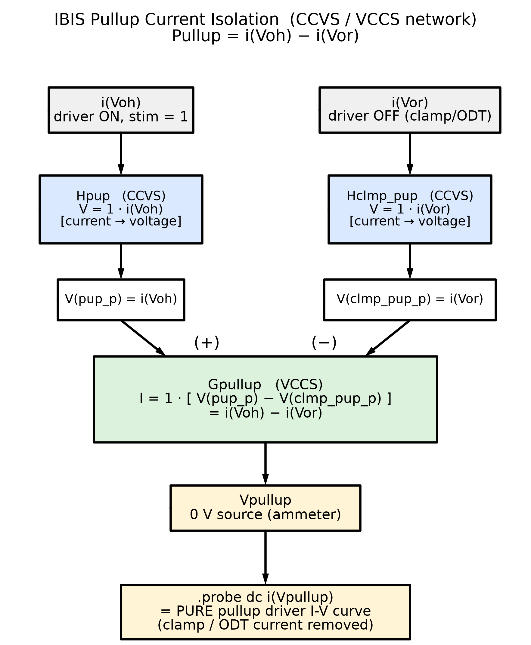
You need this post-processing only if your model has passive current paths (ESD clamps, ODT) that are active during the driver measurement. For a simple Output model with no clamp diodes, you can omit the third buffer instance and the entire CCVS/VCCS network, (as is done in the following section).
To check if post-processing is needed: With enable=1 and the pad biased at Vdd, inspect i(Vor) from the clamp instance. If i(Vor) ≈ 0 in driver mode, your model already isolates paths and post-processing is unnecessary. If i(Vor) shows significant leakage current, post-processing is needed.
Single-Ended Output: Simplified IV Deck
Output models have no enable pin or ODT, so the driver is always active. You need only two instances (pulldown and pullup). If your output model has no embedded ESD clamp paths, you do not need post-processing.
The reference deck spice_decks/iv_se_output.spi shows this simpler structure:
disp(fileread(fullfile(pwd, "spice_decks", "iv_se_output.spi")))
* IBIS Characterization: IV (DC Sweep) - Single-Ended Output
*
* This deck sweeps the pad voltage from -Vdd to 2*Vdd and measures the
* pulldown and pullup driver currents. The buffer is instantiated twice:
*   _L: stimulus=0 (pulldown active)  - measures Vol current
*   _H: stimulus=1 (pullup active)    - measures Voh current
*
* Your subcircuit must have this port order:
*   .subckt <name> vddq vssq pad vstim
*
* Required parameters on the subcircuit instance line:
*   rout   - driver output resistance (ohms)
*   cpad  - die capacitance at pad, for IBIS C_comp (F)
*   rdie  - internal die RC series resistance (ohms)
*   cdie  - internal die RC capacitance (F)
*

.include 'your_model.sp'

*--- Simulation Setup --------------------------------------------------------
.temp 25
.options post probe
.DC Vv_sweep_r -1.1 2.2 0.010

*--- Sweep Source (with 0.1-ohm isolation resistor) --------------------------
Vv_sweep_r v_sweep_r 0 DC 0.
Rol v_sweep v_sweep_r 0.1
.probe dc v(v_sweep)

*--- Supply ------------------------------------------------------------------
.param vdd = 1.1

*=============================================================================
* Pulldown Instance (_L): stimulus = 0, driver pulls pad toward GND
*=============================================================================
Vlow stim_L 0 DC 0.
Vol  v_sweep pad_L DC 0.
.probe dc i(Vol)

Vvddq_L vddq_L 0 DC 'vdd'
Vvssq_L vssq_L 0 DC 0.

Xbuf_L vddq_L vssq_L pad_L stim_L
+ your_model rout=34 cpad=0.9pF rdie=1e-3 cdie=1e-18

*=============================================================================
* Pullup Instance (_H): stimulus = 1, driver pulls pad toward Vdd
*=============================================================================
Vhigh stim_H 0 DC 1.
Voh   v_sweep pad_H DC 0.
.probe dc i(Voh)

Vvddq_H vddq_H 0 DC 'vdd'
Vvssq_H vssq_H 0 DC 0.

Xbuf_H vddq_H vssq_H pad_H stim_H
+ your_model rout=34 cpad=0.9pF rdie=1e-3 cdie=1e-18

*=============================================================================
* Post-Processing: Isolate Pullup/Pulldown from Clamp Currents
* (Only needed if your model has ESD clamp paths embedded in the driver)
*=============================================================================
* If your model has separate clamp paths, add a third "receiver-only"
* instance with driver disabled and subtract its current from _L and _H.
* See the I/O deck (iv_se_io.spi) for a complete example with CCVS/VCCS
* post-processing.

.END
Single-Ended Input: IV Deck
Input models have no driver. Only clamp and termination paths are present. A single instance with the pad swept captures all necessary IV data (GND Clamp and POWER Clamp):
disp(fileread(fullfile(pwd, "spice_decks", "iv_se_input.spi")))
* IBIS Characterization: IV (DC Sweep) - Single-Ended Input
*
* This deck sweeps the pad voltage from -Vdd to 2*Vdd and measures the
* clamp/termination current. Input models have no active driver, so only
* one instance is needed (driver disabled or not present).
*
* Your subcircuit must have this port order:
*   .subckt <name> vddq vssq pad corein
*
* Required parameters on the subcircuit instance line:
*   odt   - on-die termination resistance (ohms)
*   cpad  - die capacitance at pad, for IBIS C_comp (F)
*   rdie  - internal die RC series resistance (ohms)
*   cdie  - internal die RC capacitance (F)
*

.include 'your_model.sp'

*--- Simulation Setup --------------------------------------------------------
.temp 25
.options post probe
.DC Vv_sweep_r -1.1 2.2 0.010

*--- Sweep Source (with 0.1-ohm isolation resistor) --------------------------
Vv_sweep_r v_sweep_r 0 DC 0.
Rol v_sweep v_sweep_r 0.1
.probe dc v(v_sweep)

*--- Supply ------------------------------------------------------------------
.param vdd = 1.1

*=============================================================================
* Receiver Instance: measures GND clamp + POWER clamp + ODT current
*=============================================================================
Vor v_sweep pad DC 0.
.probe dc i(Vor)

Vvddq vddq 0 DC 'vdd'
Vvssq vssq 0 DC 0.
Rcore corein 0 1Meg

Xbuf vddq vssq pad corein
+ your_model odt=50 cpad=0.9pF rdie=1e-3 cdie=1e-18

.END
VT Deck: Transient Waveforms
The VT simulation captures the buffer's dynamic switching behavior. You drive the buffer with a digital stimulus and record the output voltage into a 50-ohm fixture load. IBIS requires waveforms into two fixture conditions:
GND fixture: 50 ohm from pad to ground. Captures the voltage swing range when the load terminates low.
VDD fixture: 50 ohm from pad to Vdd. Captures the voltage swing range when the load terminates high.
IBIS Designer uses the VT data to generate the [Rising Waveform] and [Falling Waveform] tables in the IBIS file. IBIS Designer also uses the VT data to compute Ramp (dV/dt at the 20%-80% crossing).
Key VT Deck Elements
PWL stimulus: A piece-wise linear source provides clean digital edges with a defined transition time. The low-high-low-high pattern ensures you capture both rising and falling edges:
Vv_stimulus v_stimulus 0
+ pwl(0 0  29ps 1  25ns 1  25.029ns 0  50ns 0  50.029ns 1  75ns 1)
The 29 ps transition time in the PWL is the full 0% to 100% rise/fall time (corresponding to roughly 17 ps for a 20%-80% measurement) and represents the input signal slew. The 25 ns hold time between edges allows the output to settle fully before the next transition.
Stimulus amplitude: scale it if your model needs it. The PWL swings 0 V to 1 V, matching the default digital stimulus that Signal Integrity Toolbox uses (0 to 1). The reference behavioral models accept this directly: their internal Edata element maps the 0→1 control range onto vol→voh. Transistor-level and other real buffer models, however, usually expect the digital input to swing rail-to-rail (0 to Vdd). If yours does, either scale the high breakpoints to your supply (pwl(0 0 29ps 'vdd' 25ns 'vdd' 25.029ns 0 50ns 0 50.029ns 'vdd' 75ns 'vdd')) or add a scaling wrapper inside your subcircuit that maps the 0→1 stimulus to your model's required input levels. The characterization methodology is unchanged; only the stimulus amplitude that your specific model's input stage expects may differ.
Transient analysis: Run the simulation for 75 ns to capture two complete cycles:
.tran 10ps 75ns
The 10 ps timestep provides adequate resolution for sub-100 ps edges.
Fixture load: A 50-ohm resistor from the pad to the fixture voltage. IBIS Designer assumes a 50-ohm fixture during VT extraction, so your deck must use 50 ohms:
Rfix_gnd pad_gnd fix_gnd 50.
Vfix_gnd fix_gnd 0 DC 0.
IBIS Designer hardcodes the 50-ohm fixture value. Use 50 ohms in your VT decks so the extraction aligns with your simulation setup.
Single-Ended I/O: VT Deck
The I/O VT deck enables the driver (enable=1) and uses two DUT instances, one per fixture condition. Both instances see the same stimulus:
disp(fileread(fullfile(pwd, "spice_decks", "vt_se_io.spi")))
* IBIS Characterization: VT (Transient) - Single-Ended I/O
*
* This deck measures the I/O buffer output voltage vs. time when switching
* into a 50-ohm fixture load. The buffer is put in driver mode (enable=1).
* Two fixture configurations are used:
*   - GND fixture: 50 ohm to ground
*   - VDD fixture: 50 ohm to Vdd
*
* The PWL stimulus drives two full cycles: low-high-low-high to capture
* both rising and falling edges.
*
* Your subcircuit must have this port order:
*   .subckt <name> vddq vssq pad vstim enable corein
*
* Required parameters on the subcircuit instance line:
*   rout   - driver output resistance (ohms)
*   odt   - on-die termination resistance (ohms)
*   cpad  - die capacitance at pad, for IBIS C_comp (F)
*   rdie  - internal die RC series resistance (ohms)
*   cdie  - internal die RC capacitance (F)
*

.include 'your_model.sp'

*--- Simulation Setup --------------------------------------------------------
.temp 25
.options post probe
.tran 10ps 75ns

*--- Stimulus (PWL with 29ps edges) ------------------------------------------
Vv_stimulus v_stimulus 0
+ pwl(0 0  29ps 1  25ns 1  25.029ns 0  50ns 0  50.029ns 1  75ns 1)
.probe tran v(v_stimulus)

*--- Supply ------------------------------------------------------------------
.param vdd = 1.1

*=============================================================================
* GND Fixture Instance: 50 ohm to ground, enable=1 (driver mode)
*=============================================================================
.probe tran v(pad_gnd)

Vvddq_gnd vddq_gnd 0 DC 'vdd'
Vvssq_gnd vssq_gnd 0 DC 0.
Ven_gnd   en_gnd   0 DC 1.
Vfix_gnd  fix_gnd  0 DC 0.
Rfix_gnd  pad_gnd  fix_gnd 50.
Rcore_gnd core_gnd 0 1Meg

Xbuf_gnd vddq_gnd vssq_gnd pad_gnd v_stimulus en_gnd core_gnd
+ your_model rout=34 odt=50 cpad=0.9pF rdie=1e-3 cdie=1e-18

*=============================================================================
* VDD Fixture Instance: 50 ohm to Vdd, enable=1 (driver mode)
*=============================================================================
.probe tran v(pad_vdd)

Vvddq_vdd vddq_vdd 0 DC 'vdd'
Vvssq_vdd vssq_vdd 0 DC 0.
Ven_vdd   en_vdd   0 DC 1.
Vfix_vdd  fix_vdd  0 DC 'vdd'
Rfix_vdd  pad_vdd  fix_vdd 50.
Rcore_vdd core_vdd 0 1Meg

Xbuf_vdd vddq_vdd vssq_vdd pad_vdd v_stimulus en_vdd core_vdd
+ your_model rout=34 odt=50 cpad=0.9pF rdie=1e-3 cdie=1e-18

.END
Single-Ended Output: VT Deck
Identical structure to the I/O deck but without the enable and corein ports:
disp(fileread(fullfile(pwd, "spice_decks", "vt_se_output.spi")))
* IBIS Characterization: VT (Transient) - Single-Ended Output
*
* This deck measures the buffer output voltage vs. time when switching
* into a 50-ohm fixture load. Two instances are needed:
*   - GND fixture: 50 ohm to ground (captures rising/falling into low-Z)
*   - VDD fixture: 50 ohm to Vdd   (captures rising/falling into high-Z)
*
* The PWL stimulus drives two full cycles: low-high-low-high to capture
* both rising and falling edges. Edge rate = 29ps (0%-100% transition time; ~17ps for 20%-80%).
*
* Your subcircuit must have this port order:
*   .subckt <name> vddq vssq pad vstim
*
* Required parameters on the subcircuit instance line:
*   rout   - driver output resistance (ohms)
*   cpad  - die capacitance at pad, for IBIS C_comp (F)
*   rdie  - internal die RC series resistance (ohms)
*   cdie  - internal die RC capacitance (F)
*

.include 'your_model.sp'

*--- Simulation Setup --------------------------------------------------------
.temp 25
.options post probe
.tran 10ps 75ns

*--- Stimulus (PWL with 29ps edges) ------------------------------------------
Vv_stimulus v_stimulus 0
+ pwl(0 0  29ps 1  25ns 1  25.029ns 0  50ns 0  50.029ns 1  75ns 1)
.probe tran v(v_stimulus)

*--- Supply ------------------------------------------------------------------
.param vdd = 1.1

*=============================================================================
* GND Fixture Instance: 50 ohm to ground
* Probes: v(pad_gnd) is the VT waveform for the GND fixture
*=============================================================================
.probe tran v(pad_gnd)

Vvddq_gnd vddq_gnd 0 DC 'vdd'
Vvssq_gnd vssq_gnd 0 DC 0.
Vfix_gnd  fix_gnd  0 DC 0.
Rfix_gnd  pad_gnd  fix_gnd 50.

Xbuf_gnd vddq_gnd vssq_gnd pad_gnd v_stimulus
+ your_model rout=34 cpad=0.9pF rdie=1e-3 cdie=1e-18

*=============================================================================
* VDD Fixture Instance: 50 ohm to Vdd
* Probes: v(pad_vdd) is the VT waveform for the VDD fixture
*=============================================================================
.probe tran v(pad_vdd)

Vvddq_vdd vddq_vdd 0 DC 'vdd'
Vvssq_vdd vssq_vdd 0 DC 0.
Vfix_vdd  fix_vdd  0 DC 'vdd'
Rfix_vdd  pad_vdd  fix_vdd 50.

Xbuf_vdd vddq_vdd vssq_vdd pad_vdd v_stimulus
+ your_model rout=34 cpad=0.9pF rdie=1e-3 cdie=1e-18

.END
Input Models: No VT Deck Required
Input models have no driver, so they produce no VT waveforms. IBIS Designer does not require VT files for Input model types. The IV (clamp curves) and AC (C_comp) data fully characterize the receiver.
AC Deck: Admittance for C_comp Extraction
The AC simulation measures the small-signal input admittance at the pad. IBIS Designer uses this measurement to extract C_comp (the total die capacitance). You measure at a single frequency: 100 MHz.
Key AC Deck Elements
Single-frequency AC analysis:
.ac poi 1 100meg
The poi 1 specifies one frequency point. 100 MHz is the conventional frequency for IBIS C_comp extraction: high enough to give a meaningful admittance reading, but low enough that transmission-line effects are negligible. The IBIS model records only the extracted capacitance, not the frequency, so IBIS Designer does not need to know the frequency you used. You can choose any reasonable frequency for your AC deck.
.net statement: This statement tells HSPICE to compute the network admittance parameters looking into the voltage source at the pad:
.net Vpad Rin=50
.probe ac yin(i)
The imaginary part of Y_in gives the susceptance. You compute C_comp from this value:
This formula applies directly to single-ended decks, where it yields the per-pin C_comp. For a differential deck the measurement captures both pads in parallel, so the raw result is twice the per-pin value; see Differential AC: Zero-Differential Bias below.
Bias point: You bias the pad at Vdd/2 (the typical DC operating point for a receiver) with a small AC stimulus:
Vpad pad 0 DC='vdd/2' AC=0.1V
Buffer state: For I/O models, you place the buffer in receiver mode (enable=0) for the standard "AC" measurement. An optional "AX" measurement with enable=1 captures the output-mode capacitance.
Single-Ended I/O: AC and AX Decks
The AC deck (receiver mode):
disp(fileread(fullfile(pwd, "spice_decks", "ac_se_io.spi")))
* IBIS Characterization: AC (Admittance) - Single-Ended I/O
*
* This deck extracts C_comp for an I/O buffer in receiver mode (enable=0).
* The pad is biased at Vdd/2 and a small AC stimulus is applied. The .net
* statement extracts input admittance.
*
* For I/O models, you may also want an "AX" (output-mode AC) deck that
* measures C_comp with the driver enabled (enable=1). See ax_se_io.spi.
*
* Your subcircuit must have this port order:
*   .subckt <name> vddq vssq pad vstim enable corein
*
* Required parameters on the subcircuit instance line:
*   rout   - driver output resistance (ohms)
*   odt   - on-die termination resistance (ohms)
*   cpad  - die capacitance at pad, for IBIS C_comp (F)
*   rdie  - internal die RC series resistance (ohms)
*   cdie  - internal die RC capacitance (F)
*

.include 'your_model.sp'

*--- Simulation Setup --------------------------------------------------------
.temp 25
.options probe csdf ingold=2

*--- AC Analysis: single frequency point at 100 MHz --------------------------
.ac poi 1 100meg
.probe ac yin(i)
.net Vpad Rin=50

*--- Supply ------------------------------------------------------------------
.param vdd = 1.1

*=============================================================================
* I/O Instance: receiver mode (enable=0), pad biased at Vdd/2
*=============================================================================
Vvddq vddq 0 DC 'vdd'
Vvssq vssq 0 DC 0.
Ven   en   0 DC 0.
Vpad  pad  0 DC='vdd/2' AC=0.1V
Vstim stim 0 DC 0.
Rcore corein 0 1Meg

Xbuf vddq vssq pad stim en corein
+ your_model rout=34 odt=50 cpad=0.9pF rdie=1e-3 cdie=1e-18

.END
The AX deck (driver mode, optional):
disp(fileread(fullfile(pwd, "spice_decks", "ax_se_io.spi")))
* IBIS Characterization: AX (Output-Mode AC) - Single-Ended I/O
*
* This deck extracts C_comp for an I/O buffer in driver mode (enable=1).
* The "AX" measurement is optional but provides a more accurate C_comp
* value for the output state (driver FETs contribute gate/drain capacitance
* differently when enabled vs. disabled).
*
* Your subcircuit must have this port order:
*   .subckt <name> vddq vssq pad vstim enable corein
*
* Required parameters on the subcircuit instance line:
*   rout   - driver output resistance (ohms)
*   odt   - on-die termination resistance (ohms)
*   cpad  - die capacitance at pad, for IBIS C_comp (F)
*   rdie  - internal die RC series resistance (ohms)
*   cdie  - internal die RC capacitance (F)
*

.include 'your_model.sp'

*--- Simulation Setup --------------------------------------------------------
.temp 25
.options probe csdf ingold=2

*--- AC Analysis: single frequency point at 100 MHz --------------------------
.ac poi 1 100meg
.probe ac yin(i)
.net Vpad Rin=50

*--- Supply ------------------------------------------------------------------
.param vdd = 1.1

*=============================================================================
* I/O Instance: driver mode (enable=1), stimulus=0 (pulldown active)
* Pad biased at Vdd/2 for small-signal measurement
*=============================================================================
Vvddq vddq 0 DC 'vdd'
Vvssq vssq 0 DC 0.
Ven   en   0 DC 1.
Vpad  pad  0 DC='vdd/2' AC=0.1V
Vstim stim 0 DC 0.
Rcore corein 0 1Meg

Xbuf vddq vssq pad stim en corein
+ your_model rout=34 odt=50 cpad=0.9pF rdie=1e-3 cdie=1e-18

.END
Single-Ended Input: AC Deck
disp(fileread(fullfile(pwd, "spice_decks", "ac_se_input.spi")))
* IBIS Characterization: AC (Admittance) - Single-Ended Input
*
* This deck extracts C_comp (die capacitance) from a single-frequency
* AC admittance measurement. The pad is biased at Vdd/2 (the typical
* operating point) and a small AC stimulus is applied. The .net statement
* extracts input admittance, from which C_comp is computed as:
*
*   C_comp = imag(Y_in) / (2*pi*f)
*
* Your subcircuit must have this port order:
*   .subckt <name> vddq vssq pad corein
*
* Required parameters on the subcircuit instance line:
*   odt   - on-die termination resistance (ohms)
*   cpad  - die capacitance at pad, for IBIS C_comp (F)
*   rdie  - internal die RC series resistance (ohms)
*   cdie  - internal die RC capacitance (F)
*

.include 'your_model.sp'

*--- Simulation Setup --------------------------------------------------------
.temp 25
.options probe csdf ingold=2

*--- AC Analysis: single frequency point at 100 MHz --------------------------
.ac poi 1 100meg
.probe ac yin(i)
.net Vpad Rin=50

*--- Supply ------------------------------------------------------------------
.param vdd = 1.1

*=============================================================================
* Receiver Instance: pad biased at Vdd/2, AC stimulus applied
*=============================================================================
Vvddq vddq 0 DC 'vdd'
Vvssq vssq 0 DC 0.
Vpad  pad  0 DC='vdd/2' AC=0.1V
Rcore corein 0 1Meg

Xbuf vddq vssq pad corein
+ your_model odt=50 cpad=0.9pF rdie=1e-3 cdie=1e-18

.END
Single-Ended Output: AC Deck
disp(fileread(fullfile(pwd, "spice_decks", "ac_se_output.spi")))
* IBIS Characterization: AC (Admittance) - Single-Ended Output
*
* This deck extracts C_comp for an Output buffer. The driver is disabled
* (stimulus held at a fixed DC level) so that only the passive die
* capacitance is measured. The pad is biased at Vdd/2.
*
* Your subcircuit must have this port order:
*   .subckt <name> vddq vssq pad vstim
*
* Required parameters on the subcircuit instance line:
*   rout   - driver output resistance (ohms)
*   cpad  - die capacitance at pad, for IBIS C_comp (F)
*   rdie  - internal die RC series resistance (ohms)
*   cdie  - internal die RC capacitance (F)
*

.include 'your_model.sp'

*--- Simulation Setup --------------------------------------------------------
.temp 25
.options probe csdf ingold=2

*--- AC Analysis: single frequency point at 100 MHz --------------------------
.ac poi 1 100meg
.probe ac yin(i)
.net Vpad Rin=50

*--- Supply ------------------------------------------------------------------
.param vdd = 1.1

*=============================================================================
* Output Instance: driver disabled (stimulus=DC), pad biased at Vdd/2
*=============================================================================
Vvddq vddq 0 DC 'vdd'
Vvssq vssq 0 DC 0.
Vpad  pad  0 DC='vdd/2' AC=0.1V
Vstim stim 0 DC 0.

Xbuf vddq vssq pad stim
+ your_model rout=34 cpad=0.9pF rdie=1e-3 cdie=1e-18

.END
Differential Testbenches
Differential buffers require additional testbench complexity to maintain proper common-mode behavior during simulation. The key difference from single-ended decks: when you sweep or stimulate one pad, the complementary pad (pad_n) must respond correctly. You cannot ground it or leave it floating.
Common-Mode Tracking (GCM) Circuit
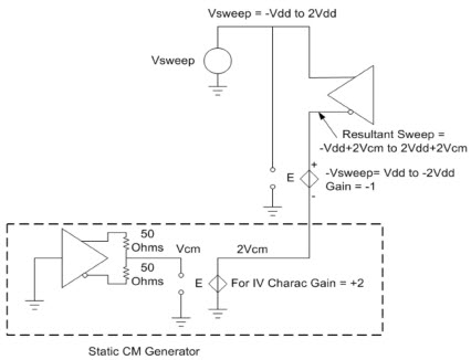
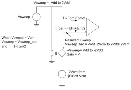
For differential IV decks, use the common-mode tracking circuit with E-sources (voltage-controlled voltage sources):
E_GCM     pad_n  GCMx2  pad 0 -1
E_GCMx2   GCMx2    0      VCM 0  2
This circuit creates the relationship pad_n = 2*VCM - pad. This means pad_n tracks as the differential complement of pad around the common-mode voltage. When you sweep pad from -Vdd to 2Vdd, pad_n simultaneously sweeps from 2Vdd down to -Vdd (in the opposite direction).
Differential Driver IV extraction circuit: static common-mode voltage generator with center-tapped 100-ohm termination and E-source tracking:
GCM Companion Instance
In addition to the E-source tracking on the swept DUT, you add a second "GCM companion" DUT instance to provide realistic common-mode loading. The companion has its stimulus fixed at 0, and you load both pads through 50-ohm resistors to a common-mode voltage node:
Rgcm     pad_gcm     VCM 50.
Rgcm_n pad_gcm_n VCM 50.
Xbuf_gcm ... stim_gcm ...
This companion establishes the common-mode reference voltage that the E-source tracking circuit uses. Without it, the VCM node floats.
Differential Receiver IV extraction circuit: common-mode voltage established by the GCM companion instance (through its center-tapped 50-ohm loading) for accurate clamp current measurement:
Differential VT: Dual-Instance Architecture
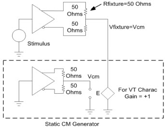
Differential VT decks use a different approach than IV. Instead of E-source tracking, you run two complete DUT instances simultaneously:
VCM instance (signal): You drive it with the PWL stimulus and load it through 50-ohm resistors to a VCM fixture node.
GCM instance (companion): Stimulus=0. You load it through 50-ohm resistors to a GCM fixture node.
An E-source ties the VCM fixture voltage to track the GCM fixture voltage:
E_VCM VCM 0 GCM 0 1
The fixture termination voltage for the driven instance tracks whatever common-mode the companion pair settles to. This maintains proper differential operation throughout the switching transition.
Differential Driver VT extraction circuit: GCM companion at center-tap of 100-ohm termination provides common-mode fixture voltage:
Differential AC: Zero-Differential Bias
In differential AC decks, you place a simple voltage source between pad and pad_n to force equal voltage on both (zero differential). You then measure the common-mode admittance:
Vdif_pad pad pad_n DC 0V
Note on the differential C_comp value. Because Vdif_pad ties the two pads together, it acts as an AC short between them, so the measured admittance includes both pad capacitors in parallel. The raw is therefore twice the per-pin C_comp. IBIS Designer accounts for this automatically and extracts the correct per-pin value, so you feed it the differential AC file as-is. Only if you compute C_comp by hand from a differential .ac0 do you need to divide the result by two.
Differential I/O: IV Deck
This is the most complex deck. You use three DUT instances (pulldown, pullup, clamp), each with its own GCM companion and common-mode tracking.
disp(fileread(fullfile(pwd, "spice_decks", "iv_diff_io.spi")))
* IBIS Characterization: IV (DC Sweep) - Differential I/O
*
* This deck sweeps the pad voltage from -Vdd to 2*Vdd and measures:
*   - Pulldown current (Vol): driver enabled, stimulus=0
*   - Pullup current (Voh):   driver enabled, stimulus=1
*   - Clamp/ODT current (Vor): driver disabled (receiver mode)
*
* Each DUT instance has common-mode tracking and a GCM companion.
* Post-processing with CCVS/VCCS isolates raw pullup/pulldown from clamps.
*
* Your subcircuit must have this port order:
*   .subckt <name> vddq vssq pad pad_n vstim enable corein
*
* Required parameters on the subcircuit instance line:
*   rout   - driver output resistance (ohms)
*   odt   - on-die termination resistance (ohms)
*   cpad  - die capacitance at pad, for IBIS C_comp (F)
*   rdie  - internal die RC series resistance (ohms)
*   cdie  - internal die RC capacitance (F)
*

.include 'your_model.sp'

*--- Simulation Setup --------------------------------------------------------
.temp 25
.options post probe
.DC Vv_sweep_r -2.0 4.0 0.010

*--- Sweep Source (with 0.1-ohm isolation resistor) --------------------------
Vv_sweep_r v_sweep_r 0 DC 0.
Rol v_sweep v_sweep_r 0.1
.probe dc v(v_sweep)

*--- Supply ------------------------------------------------------------------
.param vdd = 2.0

*=============================================================================
* Pulldown Instance (_L): enable=1, stimulus=0
*=============================================================================
Vlow stim_L 0 DC 0.
Vol  v_sweep pad_L DC 0.
.probe dc i(Vol)
Vstim_L_gcm stim_L_gcm 0 DC 0.

Vvddq_L vddq_L 0 DC 'vdd'
Vvssq_L vssq_L 0 DC 0.
Ven_L   en_L   0 DC 1.
Rcore_L core_L 0 1Meg

* Common-mode tracking
E_GCM_L     pad_L_n    GCMx2_L  pad_L 0 -1
E_GCMx2_L   GCMx2_L    0        VCM_L 0  2
.probe dc v(pad_L) v(pad_L_n)

* Swept DUT
Xbuf_L vddq_L vssq_L pad_L pad_L_n stim_L en_L core_L
+ your_model rout=50 odt=75 cpad=0.9pF rdie=1e-3 cdie=1e-18

* GCM companion
Rgcm_L     pad_L_gcm     VCM_L 50.
Rgcm_L_n   pad_L_gcm_n   VCM_L 50.
Rcore_L_gcm core_L_gcm 0 1Meg
Xbuf_L_gcm vddq_L vssq_L pad_L_gcm pad_L_gcm_n stim_L_gcm en_L core_L_gcm
+ your_model rout=50 odt=75 cpad=0.9pF rdie=1e-3 cdie=1e-18

*=============================================================================
* Pullup Instance (_H): enable=1, stimulus=1
*=============================================================================
Vhigh stim_H 0 DC 1.
Voh   v_sweep pad_H DC 0.
.probe dc i(Voh)
Vstim_H_gcm stim_H_gcm 0 DC 0.

Vvddq_H vddq_H 0 DC 'vdd'
Vvssq_H vssq_H 0 DC 0.
Ven_H   en_H   0 DC 1.
Rcore_H core_H 0 1Meg

* Common-mode tracking
E_GCM_H     pad_H_n    GCMx2_H  pad_H 0 -1
E_GCMx2_H   GCMx2_H    0        VCM_H 0  2
.probe dc v(pad_H) v(pad_H_n)

* Swept DUT
Xbuf_H vddq_H vssq_H pad_H pad_H_n stim_H en_H core_H
+ your_model rout=50 odt=75 cpad=0.9pF rdie=1e-3 cdie=1e-18

* GCM companion
Rgcm_H     pad_H_gcm     VCM_H 50.
Rgcm_H_n   pad_H_gcm_n   VCM_H 50.
Rcore_H_gcm core_H_gcm 0 1Meg
Xbuf_H_gcm vddq_H vssq_H pad_H_gcm pad_H_gcm_n stim_H_gcm en_H core_H_gcm
+ your_model rout=50 odt=75 cpad=0.9pF rdie=1e-3 cdie=1e-18

*=============================================================================
* Clamp Instance (receiver mode): enable=0
*=============================================================================
Voff  stim_R 0 DC 0.
Vor   v_sweep pad_R DC 0.
.probe dc i(Vor)
Vstim_R_gcm stim_R_gcm 0 DC 0.

Vvddq_R vddq_R 0 DC 'vdd'
Vvssq_R vssq_R 0 DC 0.
Ven_R   en_R   0 DC 0.
Rcore_R core_R 0 1Meg

* Common-mode tracking
E_GCM_R     pad_R_n    GCMx2_R  pad_R 0 -1
E_GCMx2_R   GCMx2_R    0        VCM_R 0  2
.probe dc v(pad_R) v(pad_R_n)

* Swept DUT
Xbuf_R vddq_R vssq_R pad_R pad_R_n stim_R en_R core_R
+ your_model rout=50 odt=75 cpad=0.9pF rdie=1e-3 cdie=1e-18

* GCM companion (enable=1 for the GCM to present realistic load)
Venon_R enon_R 0 DC 1.
Rgcm_R     pad_R_gcm     VCM_R 50.
Rgcm_R_n   pad_R_gcm_n   VCM_R 50.
Rcore_R_gcm core_R_gcm 0 1Meg
Xbuf_R_gcm vddq_R vssq_R pad_R_gcm pad_R_gcm_n stim_R_gcm enon_R core_R_gcm
+ your_model rout=50 odt=75 cpad=0.9pF rdie=1e-3 cdie=1e-18

*=============================================================================
* Post-Processing: Subtract clamp current from pullup/pulldown
*=============================================================================
* Pullup = i(Voh) - i(Vor)
Rpup      pup_p      0 1Meg
Rclmp_pup clmp_pup_p 0 1Meg
Hpup      pup_p      clmp_pup_n CCVS Voh 1
Hclmp_pup clmp_pup_p clmp_pup_n CCVS Vor 1
Rpullup   pullup_p   0 1Meg
Gpullup   pullup_p   pullup_n VCCS pup_p clmp_pup_p 1
Vpullup   pullup_n   0 DC 0.
.probe dc i(Vpullup)

* Pulldown = i(Vol) - i(Vor)
Rpdn      pdn_p      0 1Meg
Rclmp_pdn clmp_pdn_p 0 1Meg
Hpdn      pdn_p      clmp_pdn_n CCVS Vol 1
Hclmp_pdn clmp_pdn_p clmp_pdn_n CCVS Vor 1
Rpulldown pulldown_p 0 1Meg
Gpulldown pulldown_p pulldown_n VCCS pdn_p clmp_pdn_p 1
Vpulldown pulldown_n 0 DC 0.
.probe dc i(Vpulldown)

.END
Differential I/O: VT Deck
disp(fileread(fullfile(pwd, "spice_decks", "vt_diff_io.spi")))
* IBIS Characterization: VT (Transient) - Differential I/O
*
* This deck measures the differential I/O buffer output voltage vs. time
* when switching into a 50-ohm fixture. The buffer is in driver mode
* (enable=1). Two DUT instances are used:
*   - VCM (signal): driven by PWL stimulus
*   - GCM (companion): stimulus=0, provides common-mode pair loading
*
* Your subcircuit must have this port order:
*   .subckt <name> vddq vssq pad pad_n vstim enable corein
*
* Required parameters on the subcircuit instance line:
*   rout   - driver output resistance (ohms)
*   odt   - on-die termination resistance (ohms)
*   cpad  - die capacitance at pad, for IBIS C_comp (F)
*   rdie  - internal die RC series resistance (ohms)
*   cdie  - internal die RC capacitance (F)
*

.include 'your_model.sp'

*--- Simulation Setup --------------------------------------------------------
.temp 25
.options post probe
.tran 10ps 75ns

*--- Stimulus (PWL with 29ps edges) ------------------------------------------
Vv_stimulus v_stimulus 0
+ pwl(0 0  29ps 1  25ns 1  25.029ns 0  50ns 0  50.029ns 1  75ns 1)
.probe tran v(v_stimulus)
Vstim_gcm stim_gcm 0 DC 0.

*--- Supply ------------------------------------------------------------------
.param vdd = 2.0

*--- Common-Mode Tracking ----------------------------------------------------
E_VCM VCM 0 GCM 0 1

*=============================================================================
* VCM Instance (signal path): enable=1, driven by stimulus
*=============================================================================
Vvddq_vcm vddq_vcm 0 DC 'vdd'
Vvssq_vcm vssq_vcm 0 DC 0.
Ven_vcm   en_vcm   0 DC 1.
Rcore_vcm core_vcm 0 1Meg

Rfix_vcm     pad_vcm     VCM 50.
Rfix_vcm_n   pad_vcm_n   VCM 50.
.probe tran v(pad_vcm) v(pad_vcm_n)

Xbuf_vcm vddq_vcm vssq_vcm pad_vcm pad_vcm_n v_stimulus en_vcm core_vcm
+ your_model rout=50 odt=75 cpad=0.9pF rdie=1e-3 cdie=1e-18

*=============================================================================
* GCM Instance (companion): enable=1, stimulus=0
*=============================================================================
Vvddq_gcm vddq_gcm 0 DC 'vdd'
Vvssq_gcm vssq_gcm 0 DC 0.
Ven_gcm   en_gcm   0 DC 1.
Rcore_gcm core_gcm 0 1Meg

Rfix_gcm     pad_gcm     GCM 50.
Rfix_gcm_n   pad_gcm_n   GCM 50.
.probe tran v(GCM)

Xbuf_gcm vddq_gcm vssq_gcm pad_gcm pad_gcm_n stim_gcm en_gcm core_gcm
+ your_model rout=50 odt=75 cpad=0.9pF rdie=1e-3 cdie=1e-18

.END
Differential I/O: AC Deck
disp(fileread(fullfile(pwd, "spice_decks", "ac_diff_io.spi")))
* IBIS Characterization: AC (Admittance) - Differential I/O
*
* This deck extracts C_comp for a differential I/O buffer in receiver mode
* (enable=0). The pad is biased at Vdd/2 and Vdif_pad forces both pads
* to equal voltage for common-mode measurement.
*
* For I/O models, you may also want an "AX" (output-mode AC) deck that
* measures C_comp with the driver enabled (enable=1). See ax_diff_io.spi.
*
* Your subcircuit must have this port order:
*   .subckt <name> vddq vssq pad pad_n vstim enable corein
*
* Required parameters on the subcircuit instance line:
*   rout   - driver output resistance (ohms)
*   odt   - on-die termination resistance (ohms)
*   cpad  - die capacitance at pad, for IBIS C_comp (F)
*   rdie  - internal die RC series resistance (ohms)
*   cdie  - internal die RC capacitance (F)
*

.include 'your_model.sp'

*--- Simulation Setup --------------------------------------------------------
.temp 25
.options probe csdf ingold=2

*--- AC Analysis: single frequency point at 100 MHz --------------------------
.ac poi 1 100meg
.probe ac yin(i)
.net Vpad Rin=50

*--- Supply ------------------------------------------------------------------
.param vdd = 2.0

*=============================================================================
* Differential I/O: receiver mode (enable=0), pad biased at Vdd/2
*=============================================================================
Vvddq vddq 0 DC 'vdd'
Vvssq vssq 0 DC 0.
Ven   en   0 DC 0.
Vpad  pad  0 DC='vdd/2' AC=0.1V
Vstim stim 0 DC 0.
Rcore corein 0 1Meg

* Force equal voltage on both pads (zero differential)
Vdif_pad pad pad_n DC 0V

Xbuf vddq vssq pad pad_n stim en corein
+ your_model rout=50 odt=75 cpad=0.9pF rdie=1e-3 cdie=1e-18

.END
Differential Output: IV Deck
disp(fileread(fullfile(pwd, "spice_decks", "iv_diff_output.spi")))
* IBIS Characterization: IV (DC Sweep) - Differential Output
*
* This deck sweeps the pad voltage from -Vdd to 2*Vdd and measures the
* pulldown and pullup driver currents for a true differential buffer.
*
* Differential IV decks require common-mode tracking: as the swept pad
* voltage changes, the complementary pad (pad_n) must track at the
* opposite differential voltage around a common-mode point. This is
* achieved using an E-source (VCVS) that mirrors the pad voltage:
*
*   E_GCM pad_n GCMx2 pad 0 -1
*   E_GCMx2 GCMx2 0 VCM 0 2
*
* This ensures: pad_n = 2*VCM - pad (true complementary signal).
*
* A companion "GCM" DUT instance provides the common-mode loading that
* the swept DUT expects to see from its pair. The GCM instance has its
* stimulus fixed at 0 and is loaded through 50-ohm resistors.
*
* Your subcircuit must have this port order:
*   .subckt <name> vddq vssq pad pad_n vstim
*
* Required parameters on the subcircuit instance line:
*   rout   - driver output resistance (ohms)
*   cpad  - die capacitance at pad, for IBIS C_comp (F)
*   rdie  - internal die RC series resistance (ohms)
*   cdie  - internal die RC capacitance (F)
*

.include 'your_model.sp'

*--- Simulation Setup --------------------------------------------------------
.temp 25
.options post probe
.DC Vv_sweep_r -2.0 4.0 0.010

*--- Sweep Source (with 0.1-ohm isolation resistor) --------------------------
Vv_sweep_r v_sweep_r 0 DC 0.
Rol v_sweep v_sweep_r 0.1
.probe dc v(v_sweep)

*--- Supply ------------------------------------------------------------------
.param vdd = 2.0

*=============================================================================
* Pulldown Instance (_L): stimulus=0, with GCM tracking
*=============================================================================
Vlow stim_L 0 DC 0.
Vol  v_sweep pad_L DC 0.
.probe dc i(Vol)
Vstim_L_gcm stim_L_gcm 0 DC 0.

Vvddq_L vddq_L 0 DC 'vdd'
Vvssq_L vssq_L 0 DC 0.

* Common-mode tracking: pad_L_n = 2*VCM - pad_L
E_GCM_L     pad_L_n    GCMx2_L  pad_L 0 -1
E_GCMx2_L   GCMx2_L    0        VCM_L 0  2
.probe dc v(pad_L) v(pad_L_n)

* Swept DUT
Xbuf_L vddq_L vssq_L pad_L pad_L_n stim_L
+ your_model rout=50 cpad=0.9pF rdie=1e-3 cdie=1e-18

* GCM companion: provides common-mode loading
Rgcm_L     pad_L_gcm     VCM_L 50.
Rgcm_L_n   pad_L_gcm_n   VCM_L 50.
Xbuf_L_gcm vddq_L vssq_L pad_L_gcm pad_L_gcm_n stim_L_gcm
+ your_model rout=50 cpad=0.9pF rdie=1e-3 cdie=1e-18

*=============================================================================
* Pullup Instance (_H): stimulus=1, with GCM tracking
*=============================================================================
Vhigh stim_H 0 DC 1.
Voh   v_sweep pad_H DC 0.
.probe dc i(Voh)
Vstim_H_gcm stim_H_gcm 0 DC 0.

Vvddq_H vddq_H 0 DC 'vdd'
Vvssq_H vssq_H 0 DC 0.

* Common-mode tracking: pad_H_n = 2*VCM - pad_H
E_GCM_H     pad_H_n    GCMx2_H  pad_H 0 -1
E_GCMx2_H   GCMx2_H    0        VCM_H 0  2
.probe dc v(pad_H) v(pad_H_n)

* Swept DUT
Xbuf_H vddq_H vssq_H pad_H pad_H_n stim_H
+ your_model rout=50 cpad=0.9pF rdie=1e-3 cdie=1e-18

* GCM companion: provides common-mode loading
Rgcm_H     pad_H_gcm     VCM_H 50.
Rgcm_H_n   pad_H_gcm_n   VCM_H 50.
Xbuf_H_gcm vddq_H vssq_H pad_H_gcm pad_H_gcm_n stim_H_gcm
+ your_model rout=50 cpad=0.9pF rdie=1e-3 cdie=1e-18

.END
Differential Output: VT Deck
disp(fileread(fullfile(pwd, "spice_decks", "vt_diff_output.spi")))
* IBIS Characterization: VT (Transient) - Differential Output
*
* This deck measures the differential buffer output voltage vs. time when
* switching into a 50-ohm fixture. Two DUT instances are used:
*   - VCM (signal): driven by PWL stimulus, loaded through fixture to VCM node
*   - GCM (companion): stimulus=0, provides the common-mode pair loading
*
* The VCM fixture node voltage is set by E_VCM to track the GCM common-mode,
* ensuring proper differential operation throughout the transition.
*
* Your subcircuit must have this port order:
*   .subckt <name> vddq vssq pad pad_n vstim
*
* Required parameters on the subcircuit instance line:
*   rout   - driver output resistance (ohms)
*   cpad  - die capacitance at pad, for IBIS C_comp (F)
*   rdie  - internal die RC series resistance (ohms)
*   cdie  - internal die RC capacitance (F)
*

.include 'your_model.sp'

*--- Simulation Setup --------------------------------------------------------
.temp 25
.options post probe
.tran 10ps 75ns

*--- Stimulus (PWL with 29ps edges) ------------------------------------------
Vv_stimulus v_stimulus 0
+ pwl(0 0  29ps 1  25ns 1  25.029ns 0  50ns 0  50.029ns 1  75ns 1)
.probe tran v(v_stimulus)
Vstim_gcm stim_gcm 0 DC 0.

*--- Supply ------------------------------------------------------------------
.param vdd = 2.0

*--- Common-Mode Tracking ----------------------------------------------------
* VCM fixture termination tracks GCM common-mode voltage
E_VCM VCM 0 GCM 0 1

*=============================================================================
* VCM Instance (signal path): driven by stimulus
* Fixture: pad and pad_n each loaded through 50 ohm to VCM node
*=============================================================================
Vvddq_vcm vddq_vcm 0 DC 'vdd'
Vvssq_vcm vssq_vcm 0 DC 0.

Rfix_vcm     pad_vcm     VCM 50.
Rfix_vcm_n   pad_vcm_n   VCM 50.
.probe tran v(pad_vcm) v(pad_vcm_n)

Xbuf_vcm vddq_vcm vssq_vcm pad_vcm pad_vcm_n v_stimulus
+ your_model rout=50 cpad=0.9pF rdie=1e-3 cdie=1e-18

*=============================================================================
* GCM Instance (companion): stimulus=0, provides common-mode reference
* Fixture: pad and pad_n each loaded through 50 ohm to GCM node
*=============================================================================
Vvddq_gcm vddq_gcm 0 DC 'vdd'
Vvssq_gcm vssq_gcm 0 DC 0.

Rfix_gcm     pad_gcm     GCM 50.
Rfix_gcm_n   pad_gcm_n   GCM 50.
.probe tran v(GCM)

Xbuf_gcm vddq_gcm vssq_gcm pad_gcm pad_gcm_n stim_gcm
+ your_model rout=50 cpad=0.9pF rdie=1e-3 cdie=1e-18

.END
Differential Input: IV Deck
disp(fileread(fullfile(pwd, "spice_decks", "iv_diff_input.spi")))
* IBIS Characterization: IV (DC Sweep) - Differential Input
*
* This deck sweeps the pad voltage from -Vdd to 2*Vdd and measures the
* clamp/termination current for a true differential receiver.
*
* Common-mode tracking ensures pad_n tracks as the complement of pad.
* A GCM companion instance provides realistic common-mode loading.
*
* Your subcircuit must have this port order:
*   .subckt <name> vddq vssq pad pad_n corein
*
* Required parameters on the subcircuit instance line:
*   odt   - on-die termination resistance (ohms)
*   cpad  - die capacitance at pad, for IBIS C_comp (F)
*   rdie  - internal die RC series resistance (ohms)
*   cdie  - internal die RC capacitance (F)
*

.include 'your_model.sp'

*--- Simulation Setup --------------------------------------------------------
.temp 25
.options post probe
.DC Vv_sweep_r -2.0 4.0 0.010

*--- Sweep Source (with 0.1-ohm isolation resistor) --------------------------
Vv_sweep_r v_sweep_r 0 DC 0.
Rol v_sweep v_sweep_r 0.1
.probe dc v(v_sweep)

*--- Supply ------------------------------------------------------------------
.param vdd = 2.0

*=============================================================================
* Receiver Instance: clamp + ODT measurement with GCM tracking
*=============================================================================
Vor v_sweep pad DC 0.
.probe dc i(Vor)

Vvddq vddq 0 DC 'vdd'
Vvssq vssq 0 DC 0.
Rcore corein 0 1Meg

* Common-mode tracking: pad_n = 2*VCM - pad
E_GCM     pad_n    GCMx2  pad 0 -1
E_GCMx2   GCMx2    0      GCM_VCM 0  2
.probe dc v(pad) v(pad_n)

* Swept DUT
Xbuf vddq vssq pad pad_n corein
+ your_model odt=100 cpad=0.9pF rdie=1e-3 cdie=1e-18

* GCM companion: provides common-mode loading
Rgcm     pad_gcm     GCM_VCM 50.
Rgcm_n   pad_gcm_n   GCM_VCM 50.
Rcore_gcm corein_gcm 0 1Meg
Xbuf_gcm vddq vssq pad_gcm pad_gcm_n corein_gcm
+ your_model odt=100 cpad=0.9pF rdie=1e-3 cdie=1e-18

.END
Differential Input: AC Deck
disp(fileread(fullfile(pwd, "spice_decks", "ac_diff_input.spi")))
* IBIS Characterization: AC (Admittance) - Differential Input
*
* This deck extracts C_comp for a differential receiver. The pad is biased
* at Vdd/2 and a small AC stimulus is applied. A voltage source (Vdif_pad)
* between pad and pad_n forces both pads to the same DC voltage, so the
* measurement captures the common-mode input capacitance.
*
* Your subcircuit must have this port order:
*   .subckt <name> vddq vssq pad pad_n corein
*
* Required parameters on the subcircuit instance line:
*   odt   - on-die termination resistance (ohms)
*   cpad  - die capacitance at pad, for IBIS C_comp (F)
*   rdie  - internal die RC series resistance (ohms)
*   cdie  - internal die RC capacitance (F)
*

.include 'your_model.sp'

*--- Simulation Setup --------------------------------------------------------
.temp 25
.options probe csdf ingold=2

*--- AC Analysis: single frequency point at 100 MHz --------------------------
.ac poi 1 100meg
.probe ac yin(i)
.net Vpad Rin=50

*--- Supply ------------------------------------------------------------------
.param vdd = 2.0

*=============================================================================
* Differential Receiver: pad biased at Vdd/2, Vdif forces pad = pad_n
*=============================================================================
Vvddq vddq 0 DC 'vdd'
Vvssq vssq 0 DC 0.
Vpad  pad  0 DC='vdd/2' AC=0.1V
Rcore corein 0 1Meg

* Force equal voltage on both pads (zero differential)
Vdif_pad pad pad_n DC 0V

Xbuf vddq vssq pad pad_n corein
+ your_model odt=100 cpad=0.9pF rdie=1e-3 cdie=1e-18

.END
Corner Variation
Each deck shown above uses the typical (typ) corner configuration. To produce the three IBIS corners, run the same deck structure with modified parameter values. The following table summarizes what to change between corners. The values and percentages are only suggestions:
Parameter | Typical (typ) | Slow (min) | Fast (max) |
|---|---|---|---|
| nominal (e.g., 25) | high (e.g., 100) | low (e.g., 0) |
Vdd (supply voltage) | nominal (e.g., 1.1V) | -5% (e.g., 1.045V) | +5% (e.g., 1.155V) |
rout (driver resistance) | nominal (e.g., 34 ohm) | +10% (e.g., 37.4 ohm) | -10% (e.g., 30.6 ohm) |
odt (termination resistance) | nominal (e.g., 50 ohm) | +10% (e.g., 55 ohm) | -10% (e.g., 45 ohm) |
cpad (pad capacitance) | nominal (e.g., 0.9pF) | +5% (e.g., 0.95pF) | -5% (e.g., 0.86pF) |
SPICE model card | tt (typical-typical) | ss (slow-slow) | ff (fast-fast) |
The Vdd values shown (1.1V for single-ended, 2.0V for differential) are examples only. Replace them with your design's nominal supply voltage, and set the min/max corners to your process's actual supply tolerance.
The IBIS "min" corner represents minimum drive strength (slowest buffer):
Higher temperature increases carrier scattering, reducing mobility
Lower supply voltage reduces overdrive
Higher driver resistance directly weakens drive strength
The combination produces the slowest edges and weakest drive
The IBIS "max" corner represents maximum drive strength (fastest buffer):
Lower temperature increases carrier mobility
Higher supply voltage increases overdrive
Lower driver resistance directly strengthens drive
To create corner variants of any deck, modify these lines:
.temp 100                           $ was: .temp 25
.param vdd = 1.045                  $ was: .param vdd = 1.1
+ your_model rout=41 odt=60 cpad=0.95pf  $ was: rout=34 odt=50 cpad=0.9pf
If your SPICE model uses a separate model card for each process corner (.lib your_model.lib ss), include the appropriate library section. The exact variation percentages depend on your silicon process characterization data.
Run corner simulations for the best accuracy, but they are not required. IBIS Designer supports typical-corner-only extraction. Enable Typical corner only in the Load Files dialog box to use this mode. However, multi-corner models provide better accuracy for signal integrity simulation. Min/max corners bound the timing uncertainty that SI tools use for eye diagram analysis. If you start with typ-only and add corners later, follow the file naming convention in the next section so the IBIS Designer auto-fill can locate all files.
File Naming Convention for IBIS Designer Auto-Fill
When you produce simulation output files (CSV, .sw0, .tr0, .ac0), name them using the IBIS Designer auto-fill convention. This convention allows the tool to locate all files automatically when you browse to the output folder:
{file_type}_{corner}_{modelname}.{ext}
Where:
file_type:
iv,vt,ac, oraxcorner:
tt(typical),ss(slow),ff(fast)modelname: your model identifier (for example,
ddr5_dq_io)ext:
.csv,.sw0,.tr0,.ac0
Example file set for a complete I/O model extraction:
iv_tt_ddr5_dq_io.sw0    vt_tt_ddr5_dq_io.tr0    ac_tt_ddr5_dq_io.ac0    ax_tt_ddr5_dq_io.ac0
iv_ss_ddr5_dq_io.sw0    vt_ss_ddr5_dq_io.tr0    ac_ss_ddr5_dq_io.ac0    ax_ss_ddr5_dq_io.ac0
iv_ff_ddr5_dq_io.sw0    vt_ff_ddr5_dq_io.tr0    ac_ff_ddr5_dq_io.ac0    ax_ff_ddr5_dq_io.ac0
Required Decks per Model Type
Not all model types require all simulation types. Use this table to determine which decks you need to produce:
Model Type | IV | VT | AC (receiver) | AX (driver) |
|---|---|---|---|---|
Input | required | not needed | required | not applicable |
Output | required | required | required | not applicable |
I/O | required | required | required | optional |
For Input models, only the clamp IV and C_comp are meaningful. The model has no driver to produce VT waveforms or output-mode capacitance.
Summary of Reference Deck Files
This topic includes 18 complete reference decks in the spice_decks/ subfolder:
Model Type | Signaling | IV Deck | VT Deck | AC Deck | AX Deck |
|---|---|---|---|---|---|
I/O | Single-Ended |
|
|
|
|
I/O | Differential |
|
|
|
|
Output | Single-Ended |
|
|
| — |
Output | Differential |
|
|
| — |
Input | Single-Ended |
| — |
| — |
Input | Differential |
| — |
| — |
The spice_decks/ subfolder also contains a golden/ subfolder with correlation decks (golden_*_spice.spi). Those decks are not part of the characterization flow above; they support the golden-waveform validation described in the Correlate an IBIS Model Against Its Source SPICE Model topic. Each IBIS correlation deck is tied to a specific Model_type (I/O, Output, or Input) and must be run against a model of that same type: the B-element terminal list differs by type, and a mismatch aborts the HSPICE run. See Match the Deck to the Model Type in that topic.
Next Steps
After you run these simulations, use the IBIS Designer SPICE Simulation workflow to convert the output files into an IBIS model. See Create IBIS Model from SPICE Simulation Data.
For early-stage design exploration without SPICE data, see Create IBIS Model from Electrical Specifications.
Golden waveform validation: After you generate your IBIS model, create correlation decks that drive the buffer into a realistic channel (transmission line + capacitive load). Compare the SPICE waveform to an IBIS simulation of the same model and channel. This validates that the IBIS model represents the SPICE behavior. See Correlate an IBIS Model Against Its Source SPICE Model for details.

