PCBWriter
Description
Use the PCBWriter object to create a printed circuit board
(PCB) design files based on multilayer 2-D PCB design. A set of manufacturing files
known as Gerber files describes a PCB. A Gerber file uses an ASCII vector format for 2-D
binary images.
Creation
Syntax
Description
b = PCBWriter(
creates a pcbcomponentObject)PCBWriter object that generates Gerber-format PCB
design files based on a 2-D PCB design geometry using PCB stack.
b = PCBWriter(
creates a customized PCB file using specified
pcbcomponentObject,rfConnector)rfConnector type.
b = PCBWriter(
creates a customized PCB file using a specified PCB service,
pcbcomponentObject,writer)writer.
b = PCBWriter(
creates customised PCB file using specified PCB service and PCB connector
type.pcbcomponentObject,rfConnector,writer)
Input Arguments
Properties
Object Functions
gerberWrite | Generate Gerber files |
Examples
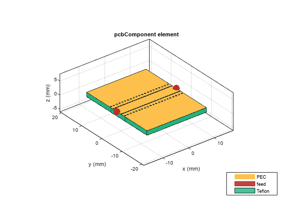
Create a coplanar waveguide.
cpw = coplanarWaveguide
cpw =
  coplanarWaveguide with properties:

              Length: 0.0231
               Width: 0.0039
             Spacing: 2.0000e-04
          ViaSpacing: [0.0011 0.0070]
         ViaDiameter: 5.0000e-04
              Height: 0.0016
    GroundPlaneWidth: 0.0300
           Substrate: [1×1 dielectric]
           Conductor: [1×1 metal]
Use this waveguide to create a pcbComponent object.
p = pcbComponent(cpw);
p.Name = 'Coplanar Waveguide'
p =
pcbComponent with properties:
Name: 'Coplanar Waveguide'
Revision: 'v1.0'
BoardShape: [1×1 antenna.Rectangle]
BoardThickness: 0.0016
Layers: {[1×1 antenna.Polygon] [1×1 dielectric] [1×1 antenna.Rectangle]}
FeedLocations: [2×4 double]
FeedDiameter: 0.0019
ViaLocations: [42×4 double]
ViaDiameter: 5.0000e-04
FeedViaModel: 'strip'
Conductor: [1×1 metal]
Tilt: 0
TiltAxis: [0 0 1]
Load: [1×1 lumpedElement]
show(p)
Use an SMA_Cinch as an RF connector and Mayhew Writer as a 3-D viewer.
c = PCBConnectors.SMA_Cinch
c =
  SMA_Cinch with properties:

                    Type: 'SMA'
                     Mfg: 'Cinch'
                    Part: '142-0711-202'
              Annotation: 'SMA'
               Impedance: 50
               Datasheet: 'https://belfuse.com/resources/Johnson/drawings/dr-142-0711-202.pdf'
                Purchase: 'https://www.digikey.com/product-detail/en/cinch-connectivity-solutions-johnson/142-0711-202/J10154TR-ND/3587681'
               TotalSize: [0.0071 0.0071]
           GroundPadSize: [0.0024 0.0024]
       SignalPadDiameter: 0.0017
         PinHoleDiameter: 0.0013
           IsolationRing: 0.0041
    VerticalGroundStrips: 1

   Cinch 142-0711-202 (Example Purchase)
s = PCBServices.MayhewWriter
s =
  MayhewWriter with properties:

               BoardProfileFile: 'legend'
          BoardProfileLineWidth: 1
                 CoordPrecision: [2 6]
                     CoordUnits: 'in'
              CreateArchiveFile: 0
                 DefaultViaDiam: 3.0000e-04
             DrawArcsUsingLines: 1
                 ExtensionLevel: 1
                       Filename: 'untitled'
                          Files: {}
         IncludeRootFolderInZip: 0
                   PostWriteFcn: @(obj)sendTo(obj)
    SameExtensionForGerberFiles: 0
                    UseExcellon: 1
Create a PCB component design file.
PW = PCBWriter(p,s,c)
PW =
  PCBWriter with properties:

                        Design: [1×1 struct]
                        Writer: [1×1 PCBServices.MayhewWriter]
                     Connector: {[1×1 PCBConnectors.SMA_Cinch]  [1×1 PCBConnectors.SMA_Cinch]}
           UseDefaultConnector: 0
    ComponentBoundaryLineWidth: 8
         ComponentNameFontSize: []
            DesignInfoFontSize: []
                          Font: 'Arial'
                     PCBMargin: 5.0000e-04
                    Soldermask: 'both'
                   Solderpaste: 1

   See info for details
Version History
Introduced in R2021b