Verify Multi-Path ADC in Architectural, Behavioral, and Circuit Domains
This example shows how to use a time-interleaved analog to digital converter (ADC) from Mixed-Signal Blockset™ to develop an offset and gain calibration engine for mismatched interleaved ADC paths. For an architectural representation of time-interleaved ADC for IBIS-AMI export, see the ADC IBIS-AMI Model Based on COM (SerDes Toolbox) and Architectural 112G PAM4 ADC-Based SerDes Model (SerDes Toolbox) examples.

Introduction
High-speed ADCs (112Gb/s and above) are now commonplace in SerDes receivers. These ADCs need to sample the incoming analog data at 64GS/s and above with an effective resolution of 5-8 bits [1,2]. This sample rate exceeds the capabilities of FLASH ADC, therefore this example uses time-interleaved ADCs: a bank of ADCs is used in a round-robin fashion to provide the required aggregate sampling rate (see the reference documentation for the Interleaved ADC block), while keeping the sampling rate of each individual ADC technologically achievable. This example uses a 4-way time-interleaved ADC as shown:

The time-interleaved ADC utilizes 4 independent ADCs: ADC[0] - ADC[3]. Each ADC has independent gain and offset error parameter values. When left uncompensated these errors reduce the overall ADC effective number of bits (ENOB). The next section evaluates the impact of offset and gain errors using a Simulink® model with a time-interleaved ADC from Mixed Signal Blockset.
Open Project and Model
Open the provided ADC project, which opens the multipath_adc.slx model.
openProject('multipath_adc_proj');
Evaluate ADC in Simulink
Choose between a single frequency sinusoid and a Gaussian noise source as input to the ADC. The ADC samples the input, at regular intervals, as defined by the sampling clock source. To apply no compensation, set the offset and gain calibration parameters (oc and gc) to 0 and 1 respectively.
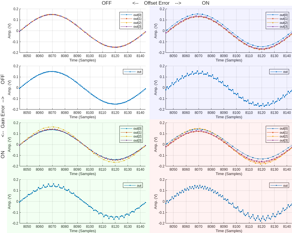
To visualize how gain and offset mismatches between time-interleaved ADCs affect the linearity of the overall time-interleaved ADC, use the provided run_adc_eval script in the scripts folder. This script generates plots for four cases: ideal, offset mismatched, gain mismatch, and offset and gain mismatched time-interleaved ADCs. The four cases are divided into four quadrants in the plots, and they are color coded as follows:
The impediment-free case (no offset and gain error) has a white background.
The case with offset, but no gain error, has a blue background.
The case with gain, but no offset error, has green background.
The case with both gain and offset errors has a red background.
set_param('multipath_adc/in_sel', 'sw', '1'); % Select input sinusoid
run_adc_eval
plot_time_domain
Notice that the output waveforms out of the independent ADCs, out[0] - out[3], appear to be correct. However, when the independent outputs are time-interleaved they no longer result in a smooth waveform, but rather have a distinct periodic signature: the signature is different for an offset-only mismatch compared to a gain-only mismatch. This interleaving induced gain/offset noise deteriorates the signal-to-noise-and-distortion ratio (SNDR).
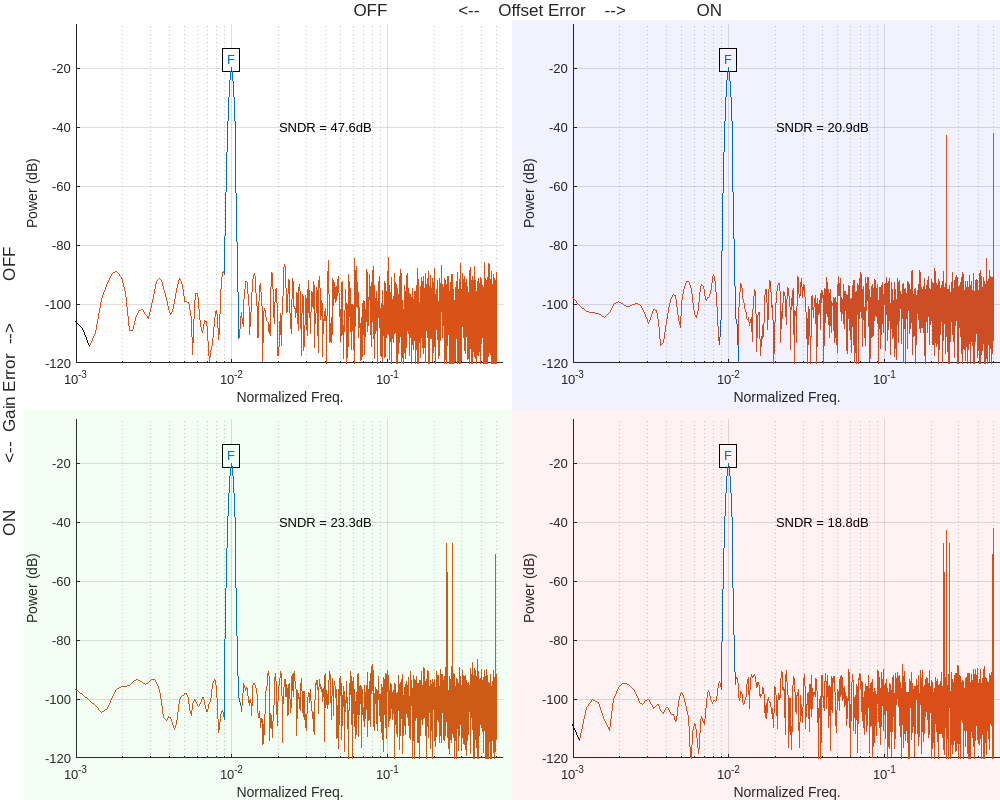
plot_spectrums
The spectrum for the time-interleaved output, for the 4 different cases, is plotted above using the background coloring scheme. The mismatch-free case has a single tone, corresponding to the input sinusoid, and a noise floor below -80dB. The noise floor amplitude is directly tied to the quantization noise of the ADC, which is determined by the resolution of the ADC. The SNDR can be mapped to the effective number of bits (ENOB) of an ADC by using the following formula:
The SNDR for the mismatch free case is 47.6dB, which maps to an ENOB of 7.6b. Notice, this is shy of the expected 8b, but we're also using an input signal that is 75% of full-scale (FS) or -2.5dB. Hence, the actual SNDR is closer to 50dB, and the expected 8b ENOB.
Offset and gain mismatches cause a degradation in the ENOB. Notice that for the offset mismatch case the SNDR is 20.9dB, for the gain mismatch case it is 23.3dB and it is 18.8dB for the gain and offset mismatch case: corresponding to an ENOB of 3.2, 3.6, and 2.8b. Hence, the 8b ADC performs like a 3b ADC if uncompensated gain and offset mismatches are present between the interleaved ADC paths.
Gain and Offset Compensation Primer
You can model the offset and gain mismatch between ADC paths in a time-interleaved ADC as an input-referred offset error and an input-referred gain error, as shown in the figure below: oe[0] - oe[3] are the input-referred offset errors and ge[0] - ge[3] are the input-referred gain errors.
Sinusoidal tones are good inputs to measure the resulting signal distortion due to offset and gain mismatches. However, practical ADC inputs are not pure tones, especially for those in an ADC-based SerDes. The input signal has an amplitude distribution that can be modeled either as a normal or uniform distribution, depending on the severity of the channel ISI and the number of signaling levels used. After compensating for offsets in components upstream from the ADC (see Verify SerDes Toolbox CTLE in Architectural, Behavioral, and Circuit Domains (SerDes Toolbox) example), the incoming signal has a zero-mean distribution (0V signal). However, in the presence of path-dependent offset and gain mismatches, the code-word distributions, as seen by each ADC path, no longer have zero mean nor equal power.
You can simulate the shift in the path dependent output mean and standard deviation by using the same script used to qualify the time-interleaved ADC performance under a sinusoidal input, but with the input switched to the random noise generator.
First, double click on the manual input switch to change it from a sinusoidal generator to a random-noise generator. Then re-run the run_adc_eval script. With the input source changed, the script generates sample distribution plots for four cases: ideal, offset mismatched, gain mismatch, and offset and gain mismatched time-interleaved ADCs.
set_param('multipath_adc/in_sel', 'sw', '0'); % Select input random-noise generator
run_adc_eval
plot_histograms
Notice that the mean () and standard-deviation () are equal for the 4 ADCs (top-left 4 histograms) when there is no gain or offset mismatch between the ADCs. However, for the other 3 cases the means and/or standard deviations are different, between the ADC paths, depending on whether the offsets and/or gains are mismatched. The mean (offset) and standard-deviation (gain) discrepancies enable a way to quantify the path discrepancies and allow for compensation using a feedback loop.
Compensation System
Now that you have a method of sensing the multi-path gain and offset errors, you need a method to correct them: the actuator. This can be done prior to analog-to-digital conversion, as shown in the figure below, in the analog domain, or after conversion in the digital domain. This example compensates for the gain and offset mismatches in the analog domain, via path independent controls for each ADC, as shown in the figure below. Here, oc[0:3] are the offset correction and gc[0:3] are the gain correction terms that will be applied.
Even though a practical ADC requires gain and offset calibration, either at power-up or periodically during mission mode, the SerDes system model likely does not model the mismatches. Yet, you can use a model for a time-interleaved ADC to test the ability of the SerDes system to compensate for gain and offset errors. The calibration algorithm is described as RTL and needs to be validated using a Verilog® simulator.
A functionally accurate, but not bit-accurate, version of a gain and offset compensation system is provided in hdl_rtl/adc_cal.v.
Offset Compensation
The RTL code fragment that compensates for the offset is shown below.
 dc[gi] = dc[gi] + (offset_en? samples[gi] : 0);
 offset[gi] = -dc[gi] / 2**atten;
When offset compensation is enabled, the signed sample value (samples[gi]) for each time-interleaved ADC path (gi) is integrated. The convergence of the offset applied to each ADC path (offset[gi]) is controlled by the bandwidth coefficient of the control feedback loop. Hence, the offset is compensated by integrating the measured average sample value, until the average sample value becomes zero mean via feedback.
The RTL code fragment that compensates for the gain mismatch is shown below.
pwr[gi] = pwr[gi] + (gain_en? - pwr[gi]/2**atten + ((samples[gi] < 0)? -samples[gi] : samples[gi])/2**atten : 0);
gain[gi] = gain[gi] + (gain_en? (tgt - pwr[gi]) / 4096 : 0);
The gain mismatch compensation loop assumes that the power of the input signal is known. It measures the average power of the independent paths using the pwr[gi] signal, one for each path. The gain compensation that is applied to each path is then the difference between the expected signal power (tgt) and the measured signal power according to the ADC path (pwr[gi]). The gain compensation settles when pwr[gi] equals the expected signal power (tgt).
Note that if the average signal power of the input signal is not known ahead of time, then it must be estimated. One method is to use the average between the individual paths as the expected signal power: . While this approach is in general more flexible, it does have a downside: the time-interleaved ADC might not have an input-to-output gain of 1. Instead, the gain-adaptation loop converges to the average of the individual path gains, rather than unity.
Generate a SystemVerilog DPI Component of the ADC
Using HDL Verifier™, generate the SystemVerilog-DPI component of the ADC with the gain error and offset error as tunable parameters using slbuild.
% Build the DPI model
set_param('multipath_adc/ADC/Interleaved ADC', 'ScalarOutput', 'off');
slbuild('multipath_adc/ADC');
Choose an HDL Simulator
Next choose an HDL simulator to run this ADC simulation along with the manually written gain and offset compensation logic. The resulting data is logged for comparison with Simulink results.
% This is a MathWorks-specific setup. You must assign PATH and
% other settings specific to your environment for your chosen simulator.
setup_questa();

% Uncomment one of the following supported HDL simulator choices:
current_hdl_simulator = 'Questa'; % Windows or Linux
% current_hdl_simulator = 'Xcelium'; % Linux only
% current_hdl_simulator = 'VCS'; % Linux only
% current_hdl_simulator = 'Vivado'; % Linux only
Compensated ADC Results
To run the ADC offset compensation algorithm, run the provided scripts/run_adc_cal_eval.m script. This script exercises the ADC offset and gain compensation algorithm in a two-step process.
First, the time-interleaved ADCs are stimulated using a signal generated from a Gaussian noise source. This input provides sufficient randomness to the input such that the ADC calibration engine can adapt the gain and offset of the independent time-interleaved ADC paths.
Next, the ADC input is switched over to a sinusoid generator, such that the distortion, resulting from the now calibrated ADC paths, can be measured.
Compensation
During the simulation, the ADC gain and offset compensation controls are logged. Traces for these are shown in the figures below for the 4 different cases: no path mismatches, only offset mismatch, only gain mismatch, both gain and offset mismatch.
run_adc_cal_eval
plot_convergence
The plot below shows the ADC calibration convergence results, both for offset and gain calibration. The initial offset/gain error is shown using a cross marker, the compensation required is shown using a circle marker, and the residual error is shown using a square marker.
plot_convergence_fit
The figures below show the resulting time-interleaved ADC ENOB, as measured after gain and offset calibration is completed. Note that in the 3 cases where there were gain and offset errors, the ENOB is restored to the ideal case after gain/offset calibration.
plot_time_domain
plot_spectrums
The output signal spectrums for the interleaved ADC show the SNDR improvement after gain and offset calibration is performed. Notice that in all 3 cases, the post-compensation SNDR is 47.2dB. This is equivalent to the offset-and-gain error free case, indicating that all interleaved paths are now in agreement.
Conclusion
The ENOB of a time-interleaved ADC can be severely degraded due to interleave path offset and gain mismatches. However, post-manufacturing calibration, either during power-up or during mission mode, can be used to sense and correct path offset and gain mismatches if the input signal characteristics are known; specifically, that the input signal is itself offset free. The use of an offset and gain compensation engine, either via analog or digital feedback, can significantly reduce the resulting ENOB degradation.
References
[1] Y. Krupnik et al., "112 Gb/s PAM4 ADC Based SERDES Receiver for Long-Reach Channels in 10nm Process," 2019 Symposium on VLSI Circuits, Kyoto, Japan, 2019, pp. C266-C267, doi: 10.23919/VLSIC.2019.8778136.
[2] E.-H. Chen and C.-K. K. Yang, "ADC-Based Serial I/O Receivers," in IEEE Transactions on Circuits and Systems I: Regular Papers, vol. 57, no. 9, pp. 2248-2258, Sept. 2010, doi: 10.1109/TCSI.2010.2071431.
[3] P. Chen, "All-Digital Calibration Algorithms for the Correction of Static Non-Linearities in ADCs," M.A.Sc. Dissertation, University of Toronto, 2020.
[4] D. Stepanovic, "Calibration Techniques for Time-Interleaved SAR A/D Converters," Ph.D. Dissertation, University of California, Berkeley, 2012.