Registered DDR3 Architectural Kit
Implement a Registered DDR3 interface for pre-layout analysis or post-layout verification.
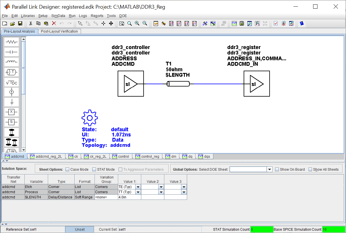
This Registered DDR3 architectural signal integrity kit includes the transfer nets, timing models, waveform processing levels and generic models for a registered DDR3 interface. This includes generic buffer models for the DDR3 controller, register and SDRAM, along with fully functional timing models and complete waveform processing levels. You can modify the kit to match your exact implementation. Then, perform complete pre-layout solution space analysis and/or full post-layout verification for waveform quality and timing margins.
Open Registered DDR3 Kit
Open the Registered DDR3 kit in the Parallel Link Designer app using the openSignalIntegrityKit function.
openSignalIntegrityKit("DDR3_Reg");
Kit Overview
For more information about the Registered DDR3 architectural signal integrity kit, including block diagrams, system configurations, transfer nets and libraries, along with instructions on how to customize the kit for a specific implementation, refer to the document DDR3_Registered.pdf that is attached to this example as a supporting file.
References
[1] JEDEC – DDR3 SDRAM Standard. JESD79-3E, July 2010.
[2] JEDEC – Definition of the SSTE32882 Registering Clock Driver with Parity and Quad Chip Selects for DDR3/DDR3L/DDR3U RDIMM 1.5V/1.35V/1.25V Applications. JESD82-29A, December 2010.
[3] JEDEC – Proposed DDR3-800/1066/1333/1600 tDS, TDH VIH.DQ, VIL.DQ and tVAC AC135 Spec. Committee: JC-42.3C. Committee Item Number: 1680.22.