Configure DDR Controller with Two Memory Designators
This example shows how you can configure a DDR controller with two custom memory designators.
Create New Project
Open the Parallel Link Designer app.
parallelLinkDesigner
Create a new project by selecting File > Project > New Project. In the newly opened dialog box, name the project as ddr2_controller, the interface as ddr2, and the schematic sheet as dq. The Pre-Layout Analysis tab shows the blank schematic sheet.
Set Up Libraries
You can create the library elements for the transmission lines, packages, connectors, and designators. In this case, you want to model a DIMM (dual in-line memory module) that has a stackup that gives a 60 ohm impedance for traces on the top and bottom layers (where the dq nets are routed). So, you need to create a 60 ohm transmission line model to be used for the transmission line segments of the DIMM.
Create T Line Model
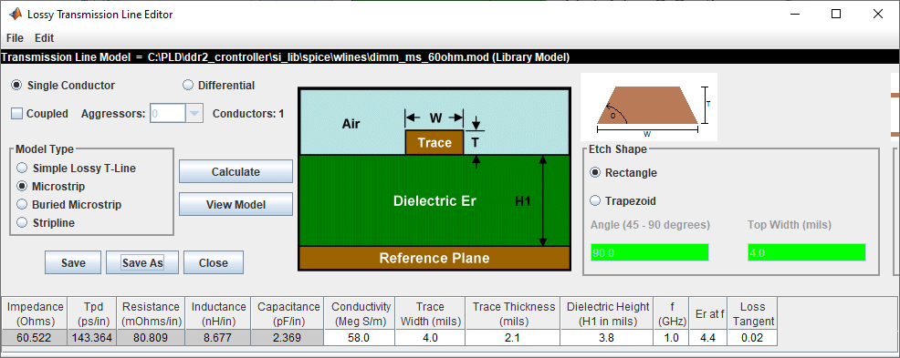
Create a differential lossy transmission line model based on a stripline cross-section. Select Tools > Lossy Transmission Line Editor. In the newly opened Lossy Transmission Line Editor dialog box, select Single Conductor and select Model Type as Microstrip. The Microstrip model type routes data lines on the top and bottom of the DIMM. The traces are 4 mils wide and 2.1 mils thick. They are 3.8 mils above a dielectric of Er 4.4. So change the parameters Trace Thickness (mils) to 2.1, Dielectric Height (H1 in mils) to 3.8, and Er at f to 4.4.
Click the Calculate button to run the 2-D field solver. The Impedance at the bottom left changes from derived to the calculated value.

Click the Save As button to save the model in the project’s library. Use the name dimm_ms_60ohm. Make sure the directory is <Project Library>/spice/wlines. Close the Lossy Transmission Line Editor.
Add Connector Model
Download the model file dimm_connector.mod attached as a supporting file to the example and copy it to the project library <project_name>/si_lib/spice/connectors.
Create Clock Domains
The bit times for the nets in the project come from the clock domain file. Edit the clock domain file by selecting Setup > Clock Domain and add the following lines:
ddr2_ck_period = 5.0
ddr2_ck_ui = ddr2_ck_period/2
ddr2_ctrl_ui = ddr2_ck_period
ddr2_addcmd_ui = 2 * ddr2_ck_period
ddr2_dq_ui = ddr2_ck_period/2
ddr2_dqs_ui = ddr2_ck_period/2
This sets the base clock period (ddr2_ck_period) to 5 ns. The data rate for all the other netclasses are set based on this rate. Changing the base clock period changes the data rate for the entire interface.
Save and close the clock domain file.
Import IBIS Models
Download and extract the IBIS_files.zip attached to this example. Select Libraries > Import IBIS and browse to the location of the downloaded files to import both ddr2 controller and sdram files.
Note that both IBIS files use the same dq_dm_sstl_18.inc file to define the 1.8V SSTL voltage levels, so you may get a Warning dialog that this file already exists. Since it is the same file, you can select either Yes or No.
Create Schematic
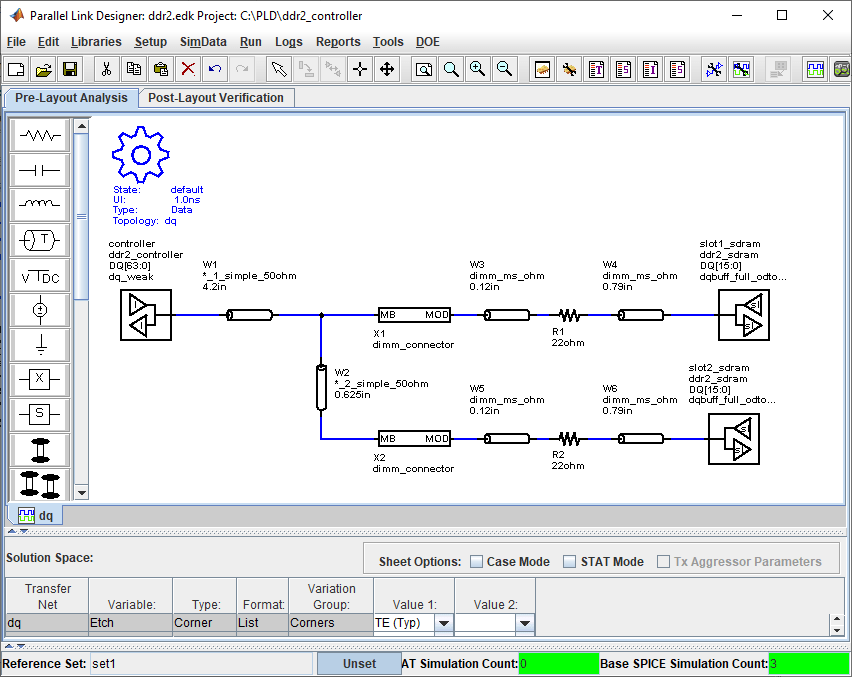
Add three single-ended designators, one controller designator on the left and two memory designators on the right. Select the controller designator on the left, right click and select Edit Designator Parts and Pins. Set the Designator parameter to controller and Part Name parameter to ddr2_controller from the dropdown menu. Since this schematic sheet represents the DQ nets, you need to add all data pins of the controller to the designator. To make it easier to select them, select Collapse Lists Into Vector Notation. Select DQ[63:0] and click the right arrow button to assign it to the designator.

Click OK to close the Edit Designator Pat/Pins dialog box.
Edit the two memory designators in the same manner as the controller. Name the top one slot1_dram and the bottom one slot2_dram. For both designators use the ddr2_sdram part and include pins DQ[15:0].
Use two lossy transmission line elements to model the etch from the controller to slot one, and the etch from slot one to slot two. Double click on the transmission lines symbols to change their lengths. Change the controller to slot one t-line length to 4.2 in and the slot one to slot two t-line length to 0.625 inches.
To add the DIMM connector models, use the subcircuit element (![]() ). In the newly opened dialog box, set the directory to
). In the newly opened dialog box, set the directory to <Project Library>\spice\connectors and select the dimm_connector.mod file. Place two connector subcircuits on the schematic, one for each DIMM.
There is a series resistor on each DIMM with a transmission line segment on each side. Add the resistor and a transmission line element. Double click and change the resistor value to 22 ohm. Right click on the transmission line element for one side of the DIMM, select Select T-Line Model from the menu, go to directory <Project Library>\spice\wlines and select dimm_ms_60ohm transmission line model that you created. Copy the resistor one more time for slot two, and the transmission line element three more times to have them both sides of the resistors. On the left side, set the transmission line segment lengths to 0.12 inch. On the right side, set the transmission line segment length to 0.79 inch. Connect the elements by double clicking on each connection to add wires to complete the schematic.

Setup Simulation and Validate Schematic
Double-click on the gear symbol (![]() ) to launch the Sheet Simulation Control dialog box. Set the UI to
) to launch the Sheet Simulation Control dialog box. Set the UI to 2.5 ns by selecting 2.5ns - ddr2_dq_ui from the dropdown menu.
In the solution space, select both slow and fast corners for etch and process corners.

Validate the schematic by selecting Run > Validate Current Schematic Set. The validation log should report no error and one warning. The warning says that the three transfer net designators have no timing data. This is telling you that there are no timing models for the controller or dram.