Prototype, Design, and Analysis of SIW based Microstrip Tapered Transmission Line
This example shows how to design and analyze a Substrate Integrated Waveguide (SIW) microstrip transmission line using Gerber files.
High performance microwave components can be designed using a novel approach called the Substrate Integrated Waveguide (SIW) technology. This approch combines the advantages of planar technology, such as low fabrication costs, with the low loss inherent to the waveguide solution.
This SIW tapered transmission line model is intended to operate in the microwave frequency range of 10GHz to 15 GHz [1] .
Define Parameters
Below is the schematic diagram of SIW based microstrip tapered transmission line model.
![]()
L   = 40.016e-3;
Wt  = 3.81e-3;
W   = 12e-3;
PW  = 2.46e-3;
L1  = 2.1e-3;
PL  = 6e-3;
gndW = W;
gndL = L+(2*L1)+(2*PL);
% define substrate
h = 0.8e-3;
sub = dielectric('Name',{'duriod'},'EpsilonR',2.2,'LossTangent',0,'Thickness',h);
Create and Analyze SIW Based Tapered Transmission Line
Use the defined parameters to create the microstrip transmisison line. A tapered section is used to match the impedance between a 50 Ω microstrip line in which quasi-TEM and TE10 mode are the dominant mode and their electric current distributions are approximate in the profile of the structure are shown.
Create the model using a pcbComponent object and visualize it using the show function.
% Create the tapered planar microstrip line trace
trace1 = traceRectangular('Length',L,'Width',W);
overlapDelta = 1e-7;
v = [-L/2+overlapDelta, Wt/2, 0; -(L/2+L1+overlapDelta), PW/2, 0; -(L/2+L1+overlapDelta),-PW/2,0;-L/2+overlapDelta, -Wt/2, 0];
trace2 = antenna.Polygon('Vertices',v);
trace3 = antenna.Polygon('Vertices',-v);
Port1  = traceRectangular('Length',PL,'Width',PW,'Center',[-gndL/2+PL/2,0]);
Port2  = traceRectangular('Length',PL,'Width',PW,'Center',[gndL/2-PL/2,0]);
Mtrace = trace1+trace2+trace3+Port1+Port2;
In order to build the PCB model, use a pcbComponent object. Mtrace created above will be the top layer on the rectangular SIW.
p = pcbComponent;
p.BoardThickness = h;
gnd = traceRectangular('Length',gndL,'Width',gndW,'Center',[0,0]);
p.BoardShape = gnd;
p.Layers = {Mtrace,sub,gnd};
Define feed and via locations. The FeedLocations and ViaLocations properties are each an array of four elements, in which the 1st and 2nd elements define the x and y co-ordinates, and the 3rd and 4th elements define the layers of connection.
% Define Feed location
p.FeedDiameter = PW/2;
p.FeedLocations = [-gndL/2,0,1,3;gndL/2,0,1,3];
p.ViaDiameter = 1e-3/2;
% Define Via location
offset = 0.5e-3;
viax = -L/2+offset;
viay = -W/2+offset;
for i=1:40
    viaSp = 0.5e-3;
    ViapointX(i) = viax + (i-1)*(viaSp)+(i-1)*(p.ViaDiameter);
    ViapointY(i) = viay;
    layer1(i) = 1;
    layer2(i) = 3;
    Viapoint1     = [ViapointX' ViapointY' layer1' layer2'];
end
for i=1:40
    viaSp = 0.5e-3;
    ViapointX1(i) = viax + (i-1)*(viaSp)+(i-1)*(p.ViaDiameter);
    ViapointY1(i) = -viay;
    layer11(i) = 1;
    layer21(i) = 3;
    Viapoint2     = [ViapointX1' ViapointY1' layer11' layer21'];
end
p.ViaLocations = [Viapoint1;Viapoint2];
figure; show(p);

Use the sparameters function to compute the s-parameters in the frequency range of 10 - 15 GHz and plot it.
freq = linspace(10e9,15e9,31);
spar = sparameters(p,freq);
figure; rfplot(spar,[2 1],1)
axis tight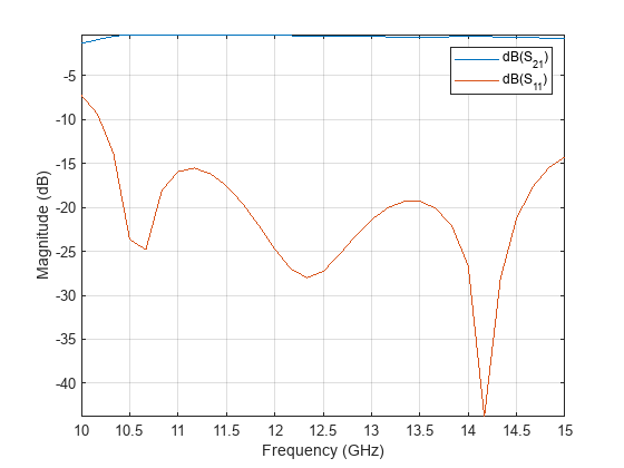
It is observed from the plot that the reflection coefficient S11 is less than -14 dB over the frequency band, and the transmission coefficient S21 is around -0.3 dB to -0.7 dB across the entire band.
Prototype the model using Gerber files
Gerber files are open ASCII vector format files that contain information on each physical board layer of the PCB design. Circuit board objects, like copper traces, vias, pads, solder mask and silkscreen images, are all represented by series of coordinates. These files are used by PCB manufacturers to translate the details of the design into the physical properties of the PCB.
To generate these files, two additional pieces of information are required apart from the PCB design. The first is the type of connector to be used and the second is the PCB manufacturing service/viewer service. The type of RF connector determines the pad layouts on the PCB. The RF PCB Toolbox™ provides a catalog of PCB services and RF connectors. The PCB services catalog supports, configuring the Gerber file generation process for manufacturing as well as for online viewer-only.
Generation of Gerber files
Gerber files contain the collection of files that describe a Printed Circuit Board (PCB) . Each file describes a specific aspect of the PCB design. For example, .gtl and .gbl files contain the information about the metal regions corresponding to the signal and ground that are filled with copper traces. Similarly, .gts and .gbs files hold the information about the solder mask, which is applied to protect and insulate the metal regions. Design information is encoded into the silkscreen layer designated by .gto and .gbo files.
To understand the generation process for these files, use a PCB manufacturing service with an online viewer and render the design.
Online viewer for Gerber files
The PCB services catalog contains different manufacturing service types that can accesed using the object PCBServices. In this example, MayhewWriter is used to configure the Gerber file generation process and view them using the Mayhewlabs free online 3D Gerber viewer. Select an SMA edge connector from the available catalog and modify it accordingly. The PCB model, PCB services, and the RF PCB connector are used to create a PCBWriter.
 s = PCBServices.MayhewWriter;
s.Filename = 'SIWMicrostripLine';
%
PW = PCBWriter(p,s);
PW.UseDefaultConnector = 0;
Using the PCBWriter created above, execute the gerberWrite command to generate the Gerber files for the SIW Model.
gerberWrite(PW)
The collection of files are generated and placed in a folder with the same name as assigned in the Filename property of the particular PCB services. This folder is located in the current working directory. The files in the folder are shown in the image below.
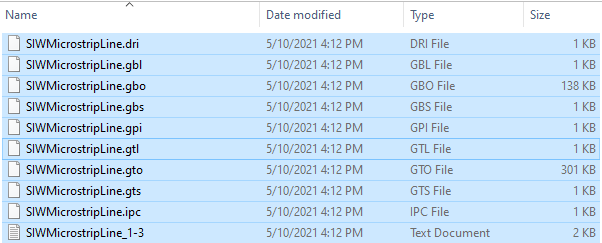
If the file name is not specified then the folder name and the files in the folder are named as "untitled".
Running the above example automatically opens up the Mayhew Labs PCB manufacturing service in the default internet browser. Further to view the 3D PCB model drag and drop the gerber files as shown below.
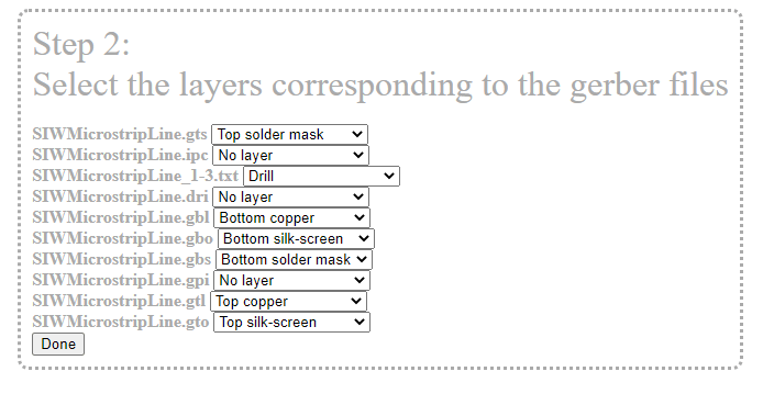
Click on Done to view the proposed PCB design as shown below.

Reference
Bouchra Rahal,et.al,"SUBSTRATE INTEGRATED WAVEGUIDE POWER DIVIDER, CIRCULATOR AND COUPLER IN [10-15] GHZ BAND", International Journal of Information Sciences and Techniques, DOI:10.5121/ijist.2014.4201 , March, 2015.