Design and Analyze HighPass Filter Using pcbComponent
This example shows how to design and analyze highpass filter using the pcbComponent object. A microstrip highpass filter is designed based on a three-pole (n = 3) Chebyshev highpass prototype with 0.1 dB passband ripple and cutoff frequency = 1.5 GHz.
Design and Analyze Highpass Filter
The element values of the corresponding low pass Chebyshev prototype are taken from Table 3.2 of reference [1]
= = 1.0
= = 1.0316
= 1.1474
Using the design equations Eqs. (6.2) and (6.3) given in reference [1] for n = 3 and = 50 ohm terminations, we can obtain quasi-lumped circuit elements values as
= = 2.0571 pF
= 4.6236 nH
A schematic diagram of such a highpass filter taken from fig 6.2 of reference [1] representing various feature dimensions is shown below. It is seen that the series capacitors and are realized by identical interdigital capacitors, while the shunt inductor is realized by a short-circuited stub. A commercial substrate (RT/D 5880) having a relative dielectric constant of 2.2 and thickness of 1.57 mm is chosen for this microstrip filter realization. The dimensions of the interdigital capacitors, such as the finger length, width, spacing between fingers, and number of the fingers are given in the fig 6.2 of reference [1]. The procedure to calculate the dimensions of interdigital capacitor and stub inductor is discussed in the section 6.1.1 of reference [1]. A closed-form design formulation for interdigital capacitor and alternatively full-wave EM simulations are used to extract desired values of lumped circuit capacitance for different feature dimensions.

Use the interdigitalCapacitor object and change its properties as per given values in reference [1] to create interdigited fingers. Visualize created object using show
idc = interdigitalCapacitor;
idc.NumFingers = 10;
idc.FingerLength = 10e-3;
idc.FingerWidth = 0.3e-3;
idc.FingerSpacing = 0.2e-3;
idc.FingerEdgeGap = 0.2e-3;
idc.GroundPlaneWidth = 5e-3;
idc.TerminalStripWidth = 0.1e-3;
idc.PortLineLength = 0.1e-3;
idc.PortLineWidth = 4.8e-3;
figure;
show(idc);

Use the pcbComponent on idc object to create a capacitor cap1. Visualize cap1 using show
pcb = pcbComponent(idc);
cap1 = pcb.Layers{1};
figure;
show(cap1);
Use the copy, rotateZ, rotateX and translate operation methods on capacitor cap1 object to create capacitor cap2. Visualize cap2 using show
cap2 = copy(cap1);
cap2 = rotateZ(cap2,180);
cap2 = rotateX(cap2,180);
cap2 = translate(cap2,[-6.2e-3 0 0]);
cap1 = translate(cap1,[6.2e-3 0 0]);
figure;
show(cap2);

Use the traceRectangular object to create both feeding ports port1, port2 and short circuited stub centerArm. Perform a Boolean add operation for the shapes port1, cap2, centerArm, cap1 and port2 to create filter. Visualize filter using show
portW = 4.9e-3;
portL = 3.6e-3;
centerL = 2e-3;
centerW = 9.9e-3;
port1 = traceRectangular(Length = portL,Width = portW,Center = [-11.4e-3-portL/2 -0.05e-3]);
port2 = traceRectangular(Length = portL,Width = portW,Center = [11.4e-3+portL/2 -0.05e-3]);

centerArm = traceRectangular(Length = centerL,Width = centerW,Center = [0 -2.55e-3]);
filter = port1 + cap2 + centerArm + cap1 + port2;
figure;
show(filter);
Define the substrate parameters and create a dielectric to use in the pcbComponent of the designed filter. Create a ground plane using the traceRectangular shape.
Use the pcbComponent to create a filter PCB. Assign the dielectric and ground plane to the Layers property on pcbComponent. Assign the FeedLocations to the edge of the feed ports. Assign ViaLocations at the edge of stub centerArm. Set the BoardThickness to 1.57 mm on the pcbComponent and visualize the filter. The below code performs these operations and creates the filter pcb object.
substrate = dielectric(EpsilonR = 2.2, LossTangent = 0.0009,...
    Name = "custom", Thickness = 1.57e-3);
gndL = 30e-3;
gndW = 25e-3;
ground = traceRectangular(Length = gndL, Width = gndW,...
    Center = [0,-4e-3]);

pcb = pcbComponent;
pcb.BoardShape = ground;
pcb.BoardThickness = 1.57e-3;
pcb.Layers ={filter,substrate,ground};
pcb.FeedDiameter = portW/2;
pcb.FeedLocations = [-gndL/2 0 1 3;gndL/2 0 1 3];
pcb.ViaDiameter = centerL;
pcb.ViaLocations = [0 -6.5e-3 1 3];
figure;
show(pcb);

Use the sparameters method to calculate the S-parameters for the highpass filter and plot it using the rfplot function.
spar = sparameters(pcb,linspace(0.1e9,3.5e9,40));
figure;
rfplot(spar);

As there are four curves in the result, let us analyze the results.
Plot S-Parameters
Analyze the values of , and to understand the behavior of highpass filter.
figure;
rfplot(spar,1,1);
hold on;
rfplot(spar,1,2);
hold on;
The result shows that the filter has -3 dB cut-off frequency = 1.8 GHz . The values are greater than -3 dB and values are less than -10 dB above -3 dB cut-off frequency 1.8 GHz. The designed filter therefore has highpass response and em simulated results matches closely with reference. The 0.3 GHz shift in -3 dB cut-off frequency might be due to use of different numerical solver.
Use the charge method to visualize the charge distribution on the metal surface and dielectric of highpass filter
figure;
charge(pcb,3e9);

figure;
charge(pcb,3e9,'dielectric');
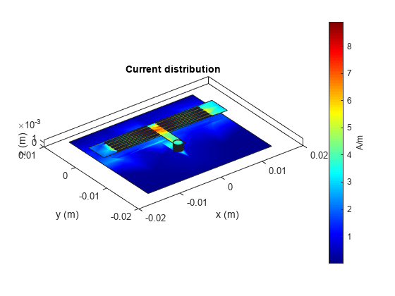
Use the current method to visualize the current distribution on the metal surface and volume polarization currents on dielectric of highpass filter
figure;
current(pcb,3e9);
figure;
current(pcb,3e9,'dielectric');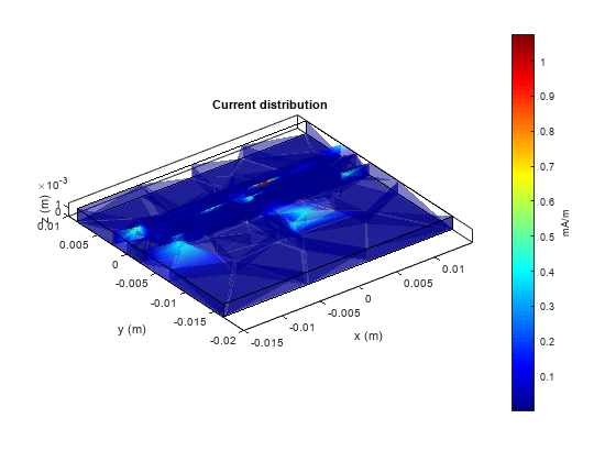
References
[1] Jia-Sheng Hong "Microstrip Filters for RF/Microwave Applications", p. 165, John Wiley & Sons, 2nd Edition, 2011.