Capture Asynchronous Data from FPGA Using Multiple FPGA Data Capture IPs
This example shows how to use multiple FPGA data capture IPs with an existing HDL design to capture the asynchronous FPGA internal signals over a JTAG connection.
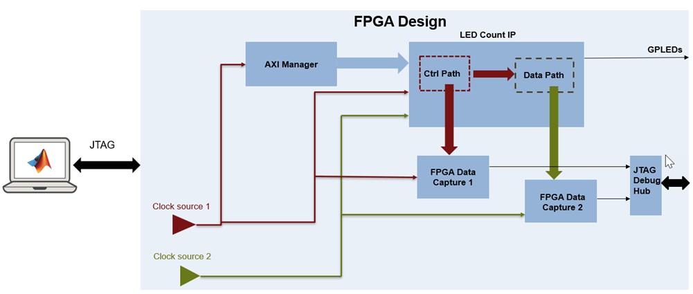
This example uses an existing HDL design that contains a LED count IP core, which blinks the LEDs on the FPGA board. The AXI Manager IP configures the LED count IP core to change the blink frequency and direction. In the HDL design, one clock source drives the AXI_Lite clock, while another clock drives the IP core clock. The example uses one data capture IP to capture the AXI_Lite signals and another one to capture the internal signals of the LED count IP core. The JTAG Debug Hub IP connects data capture IPs to host.
This example runs on ZedBoard™. You can export the design to any AMD® Zynq® board.
Requirements and Prerequisites
AMD Vivado® Design Suite, with a supported version listed in FPGA Verification Requirements
ZedBoard
JTAG cable
Prepare Example Resources
Set up the AMD Vivado tool path. This example assumes that the AMD Vivado executable is located in the C:\Xilinx\Vivado\2023.1\bin\vivado.bat file. Modify this command to use path of your AMD Vivado executable.
hdlsetuptoolpath('ToolName','Xilinx Vivado','ToolPath', ...
                 'C:\Xilinx\Vivado\2023.1\bin\vivado.bat');
Set Up FPGA Development Board
1. Confirm that the power switch is off.
2. Connect the AC power cord to the power plug and plug the power supply adapter cable into the FPGA development board.
3. Use the JTAG download cable to connect the FPGA development board with the host computer.
4. Turn on the power switch on the FPGA board.
Generate FPGA Data Capture Components
This example monitors signals from the control and data paths of the led_count_ip IP, with each path driven by two different clock sources: the control path by a 50 MHz clock and the data path by a 200 MHz clock.
In the control path, monitoring the configuration of the IP core involves observing these internal signals: AXI4_Lite_AWADDR, AXI4_Lite_AWValid, AXI4_WData, and AXI4_Lite_WValid. To facilitate this, the example taps the 32-bit tp_AXI4_Lite_AWADDR signal onto AXI4_Lite_AWADDR, the 1-bit tp_AXI4_Lite_AWValid signal onto AXI4_Lite_AWValid, the 32-bit tp_AXI4_WData signal onto AXI4_Lite_WData, and the 1-bit tp_AXI4_Lite_WValid signal onto AXI4_Lite_WValid as output ports.
In the data path, monitoring the behavior of the IP core involves observing these signals: GPLEDs, Blink_direction, and Blink_freq. To facilitate this, the example taps the 8-bit tp_GPLEDs signal onto GPLEDs, the 1-bit tp_Blink_direction signal onto Blink_direction, and the 4-bit tp_Blink_freq signal onto Blink_freq to output ports. The 8-bit tp_GPLEDs signal indicates the output of the IP core, the 1-bit tp_Blink_direction signal indicates the blink direction of LEDs, and the 4-bit tp_Blink_freq signal indicates the blinking frequency of the LEDs.
To operate on these signals over a JTAG connection, configure the data capture components by following these steps.
1. Launch the FPGA Data Capture Component Generator tool by executing this command in MATLAB®.
generateFPGADataCaptureIP
2. Set FPGA vendor to AMD.
3. Set Generated IP language to Verilog.
4. Set Connection type to JTAG.
5. Set Number of data capture IPs to 2. It creates two tabs to configure the data capture IPs.
6. Rename the first data capture IP as ctrl_path_dc and second data capture IP as data_path_dc.
7. On the Data Capture 1 tab, add four rows to the Ports table by clicking the Add button.
8. Rename the signals as AXI4_Lite_AWADDR, AXI4_Lite_AWVALID, AXI4_WDATA, and AXI4_Lite_WVALID. Change the bit widths to 32, 1, 32, and 1, respectively.
9. Set Sample depth to 128.

10. On the Data Capture 2 tab, add three rows to the Ports table by clicking the Add button.
11. Rename the signals as LED_Out, Blink_direction, and Blink_frequency. Change the bit widths to 8, 1, and 4, respectively.
12. Set Sample depth to 8192.
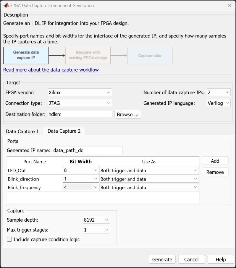
13. To generate the FPGA data capture components, click Generate. A report shows the results of the generation.
The tool generates the two subfolders under the hdlsrc folder for each data capture IP. Each subfolder contains the packaged IP core and its corresponding System object.

Integrate FPGA Data Capture HDL IPs
1. Unzip the IP core by executing this command in MATLAB.
unzip('led_count_ip_v1_0.zip');
2. Create a Vivado project for this example by executing this command in MATLAB.
system('vivado -mode batch -source leadCreateProject.tcl &')

3. Add JTAG AXI Manager IP to the user repository in Vivado project by executing this command in MATLAB.
setupAXIManagerForVivado('project_1.xpr');
4. Add the data capture IPs and the JTAG Debug Hub IP to the user repository in the Vivado project by executing this command in MATLAB.
addFPGADataCaptureToVivado('project_1.xpr','DatacaptureIPFolder','hdlsrc');

5. Open the Vivado project, add the AXI Manager, ctrl_path_dc, data_path_dc, and JTAG Debug Hub IPs to the block design and make the connections as shown below.
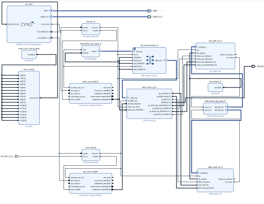
Set the address of led_count_ip_0 to 0x4A0D0000.
Alternatively, you can complete step 5 by executing this Tcl command in Vivado.
source ./ModifyLedCountPrj.tcl
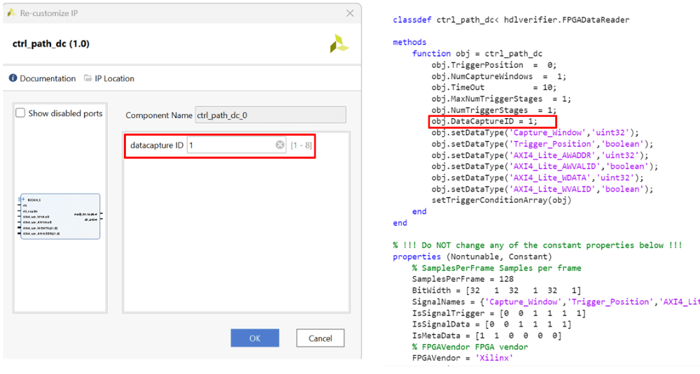
6. Make sure that the datacaptureID of each IP is unique and it matches with the corresponding System object DataCaptureID.
For example, for the ctrl_path_dc IP, you can find the System object at hdlsrc/ctrl_path_dc/ctrl_path_dc.m and DataCaptureID is 1.
Compile the design and generate the bitstream.
Wait until Vivado successfully generates the bitstream before going to the next step. This process takes approximately 5 to 10 minutes.
Capture Data
Follow these steps to capture the data.
1. Load bitstream to the targeted hardware by executing this command in MATLAB.
filProgramFPGA('AMDVivado','hdl_prj\vivado_ip_prj\vivado_prj.runs\impl_1\system_top_wrapper.bit',2)
2. Create AXI manager object in MATLAB to configure the led_count_ip IP core.
obj = aximanager('AMD');
3. Change the blinking frequency from 0 to 15. For example, set the blinking frequency to High by executing this command in MATLAB.
obj.writememory('0x400D0100',15);
4. Navigate to the directory where the FPGA data capture components are generated in MATLAB.
cd hdlsrc
Launch the FPGA Data Capture tool. This tool is customized for your data capture signals.
launchMultipleDataCaptureApp;
The above command creates a data capture hub object in the MATLAB workspace fpgadchub_obj, and launches the FPGA Data Capture tool with two tabs ctrl_path_dc and data_path_dc to configure the trigger settings for each data capture IP.
5. Run data capture IPs in non blocking mode by executing this command in MATLAB.
fpgadchub_obj.CaptureMode = 'nonblocking';
The nonblocking capture mode enables you to use FPGA data capture and AXI manager simultaneously.
6. Under each tab of data capture IP, clear Enable data capture IP if data capture is not required.
7. Configure the trigger settings of the ctrl_path_dc tab as shown below:
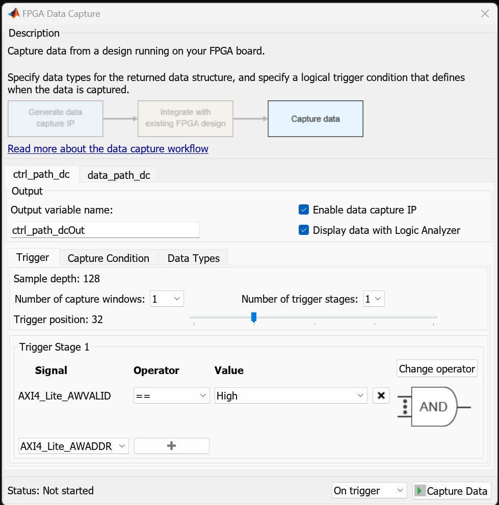
8. Configure the trigger settings of the data_path_dc tab as shown below:

9. Initiate the data capture IPs by clicking on the Capture Data button. The IPs wait for the specified trigger condition to begin the data capture process.
10. Change the blink direction by executing this command in MATLAB.
obj.writememory('0x400D0104',1);
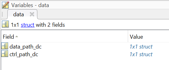
Now, data capture IPs detect the trigger condition and captures data to MATLAB workspace as ctrl_path_dcOut and data_path_dcOut structures.
The captured data is also displayed as signal waveforms in the two Logic Analyzer windows on detecting the specified trigger condition.

To capture data using command line interface, run the capture_ledblinking.m script in MATLAB.
Conclusion
This example generates multiple data capture IP cores and integrates them into an FPGA design to capture asynchronous signal data from the LED counter IP to MATLAB. You can use this example as a reference for capturing asynchronous data from your FPGA design with the aid of HDL Verifier's FPGA data capture feature.
See Also
FPGA Data Capture | dataCaptureHub | addFPGADataCaptureToVivado