Sobel Edge Detection Algorithm with Computer Vision Toolbox
This example shows and explains the "Top-Down" design methodology that is applied to Sobel Edge Detection algorithm. The Sobel Edge Detection algorithm is a popular yet simple edge detection algorithm and is the focus of this example. With this example you will learn:
How Simulink® allows you to design a digital signal processing (DSP) algorithm at a system level.
How to elaborate on the design to make it realizable in hardware.
How to co-simulate hand-written HDL code (corresponding to your Simulink model) with ModelSim® or Cadence® Xcelium™ in the Simulink environment.
This approach is an example of Model Based Design. To learn more about Model Based Design refer to https://www.mathworks.com/solutions/model-based-design.html
You need the following products to run all the models in the example:
MATLAB®
Simulink
Fixed-Point Designer™
HDL Verifier™
Computer Vision Toolbox™
DSP System Toolbox™
ModelSim SE or PE. or Cadence Xcelium
The Executable Specification of Sobel Edge Detection Algorithm
As designs become larger and more complicated, it has become necessary to describe a design at a high level. This high level description not only enables the designer to run simulations faster, it can also be used throughout the development process for verification. This resulting process allows developers to identify bugs early on and avoid costly bug discovery towards the end of development. This high-level design is usually done by system engineers.
To implement a DSP algorithm on hardware such as ASIC or an FPGA, a system level engineer first designs the algorithm and verifies that the algorithm satisfies the project requirements. This design later becomes the golden reference for the engineers responsible for taking the algorithm to the hardware.
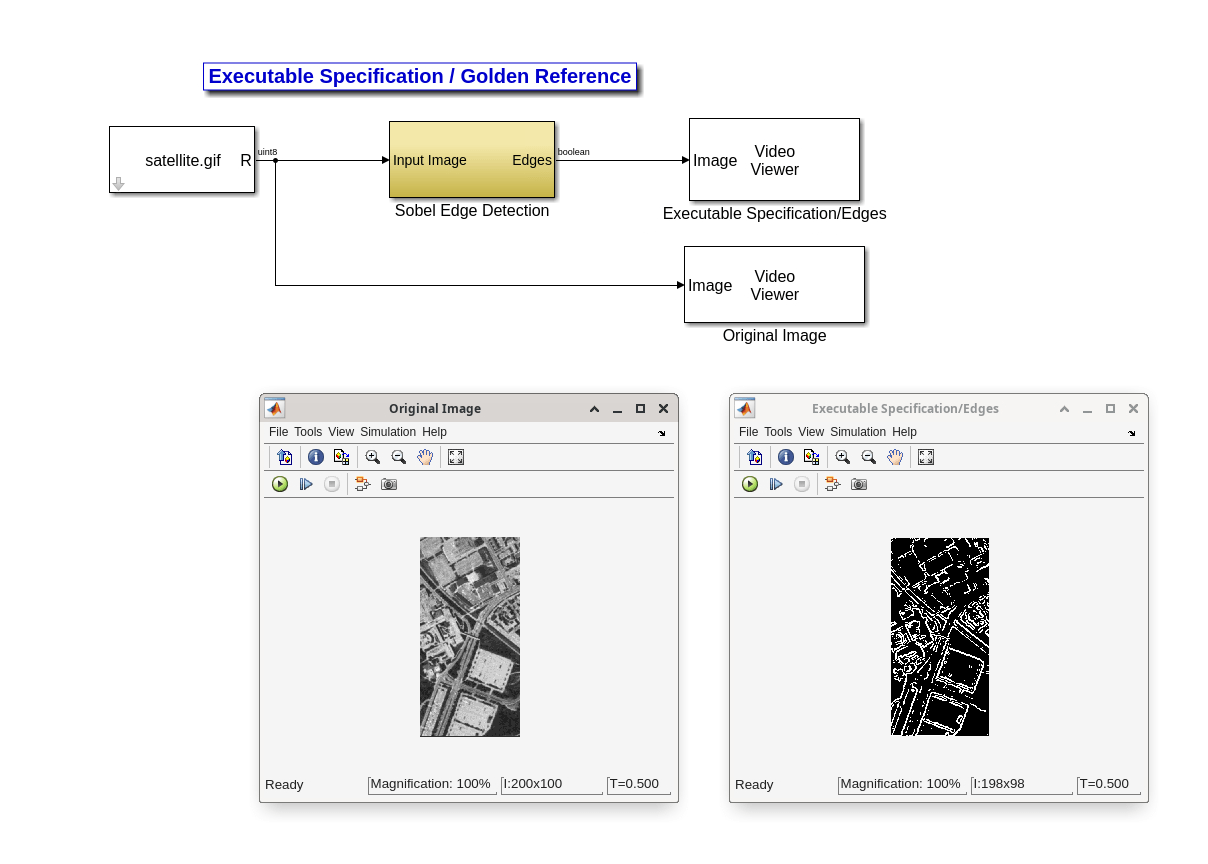
In this example, the Sobel Edge Detection algorithm has been implemented in Simulink. Open the executable model and double click on the "Sobel Edge Detection" block to learn how the algorithm is implemented in Simulink. When you double-click on the Sobel Edge Detection block, you can see that the algorithm is comprised of two 2D filters, one to calculate the gradient in the column direction (top filter) and one to calculate the gradient in the row direction (bottom filter). Both filters use a 3x3 kernel.
This Simulink model serves as the specification for the rest of the development path. It is an executable specification, meaning you can readily execute this model in the Simulink environment.
This example uses a satellite image as the input to the edge detection algorithm. This image serves as an input test vector and is used throughout the example. If engineers who are responsible for the hardware implementation of the algorithm work in the Simulink environment as well, there is no need for extra overhead in porting the test vectors into different applications or creating test harnesses that are prone to human errors. The test harness that is used in the executable specification is used throughout the example.
Design and Verification of the Algorithm for Implementation
When designing the executable model, the system engineer generally does not keep the implementation details in mind but rather implements the algorithm to match the behavioral requirements. Once the system engineer submits the executable specification to the development team, the development team may need to make modifications to the executable specification to fit the design into a real-time system that may have limited resources such as memory or processing power.
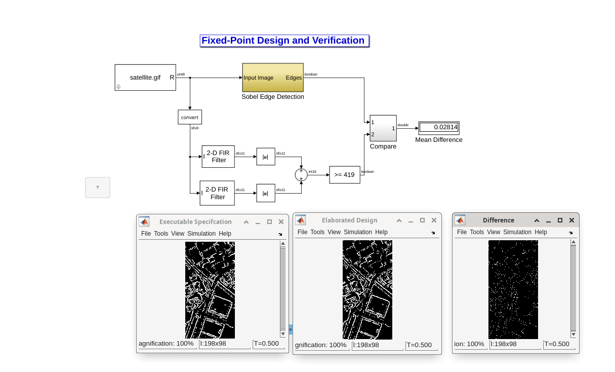
In this example, the developers may decide to eliminate the square operations and replace them with the absolute value operation for more efficient hardware implementation. This will cause a difference between the cosimulation result and the golden reference but for the sake of this example, we assume that the difference is acceptable. Open the edge detection design model. You can see the same test vectors as the previous model are still being used. The result can be easily verified against the golden reference. A numerical display shows the mean difference between the golden reference and the new design.

Fixed-Point Design
Since our ultimate goal is to implement the algorithm in an FPGA or an ASIC, we must convert our double precision design to a fixed-point design. This can be done easily using Simulink. We use the double precision model we developed in the previous section to directly develop a fixed-point model without introducing any new blocks. Simulink allows us to determine the number of bits and scaling for data as well as mathematical operations, and provides a great environment for analyzing the fixed-point operation of a system.
In this fixed-point design, the input to the filters is a signed 9-bit integer and the outputs of the filters are signed 11-bit integers. If you double-click on each computational block, such as the filters or the sum blocks, you can see that the developer can easily tune the bit width and scaling related to the internal computations of that block. This gives huge leverage to the designer to compromise between matching the output of the golden reference while using the least number of bits necessary to save area on the device.
Open the fixed-point model and examine how the fixed-point is implemented by double clicking on the computational blocks, such as the 2D filters or the addition block, and looking at the corresponding fixed-point panel.
Elaboration of the Design
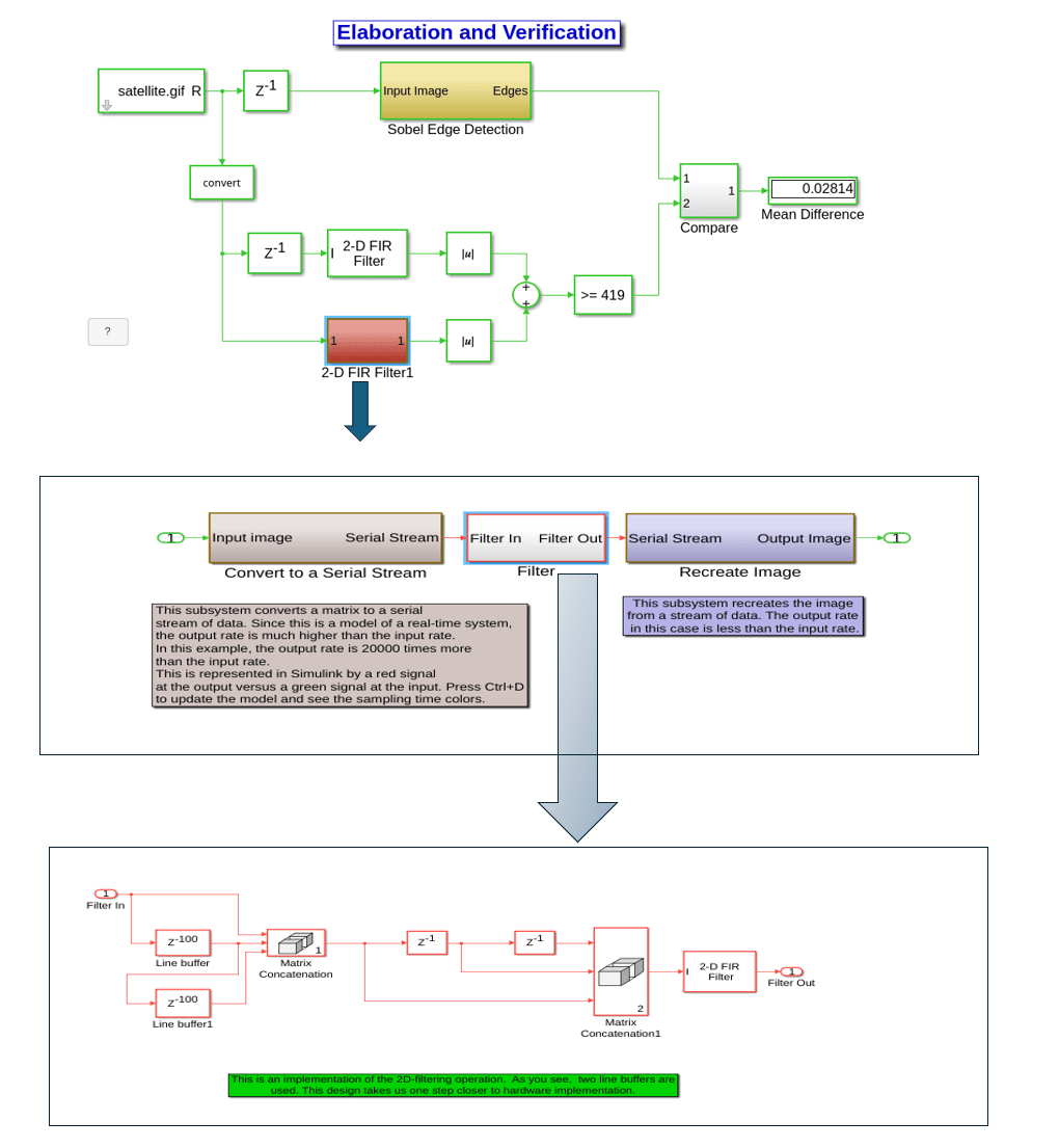
In our example, the input to the edge detection algorithm has been a two-dimensional image of size 200x100. In a real-time system, the input is most likely not a matrix but a serial stream of data; for example, this serial stream of data can be generated by a Charge-Coupled Device (CCD). Therefore, we need to modify the structure of the design such that the edge detection algorithm accepts and performs 2D filtering on a serial stream of data.
To this extent, we first serialize the input image. Then we perform the 2D filtering on this serial data. We later de-serialize the stream of data to be able to compare the output to the golden reference. To see how this is done, refer to edge detection elaboration model.
This operation is done only for the bottom filter. As expected, the new design is still producing the same exact results as before. Two delay elements have been added to compensate for the buffing in the serializer block. This design also showcases the multi-rate capability of Simulink. The output of the serializer block is 20000 times higher in sampling rate relative to the input to that block.
Simulink Cosimulation
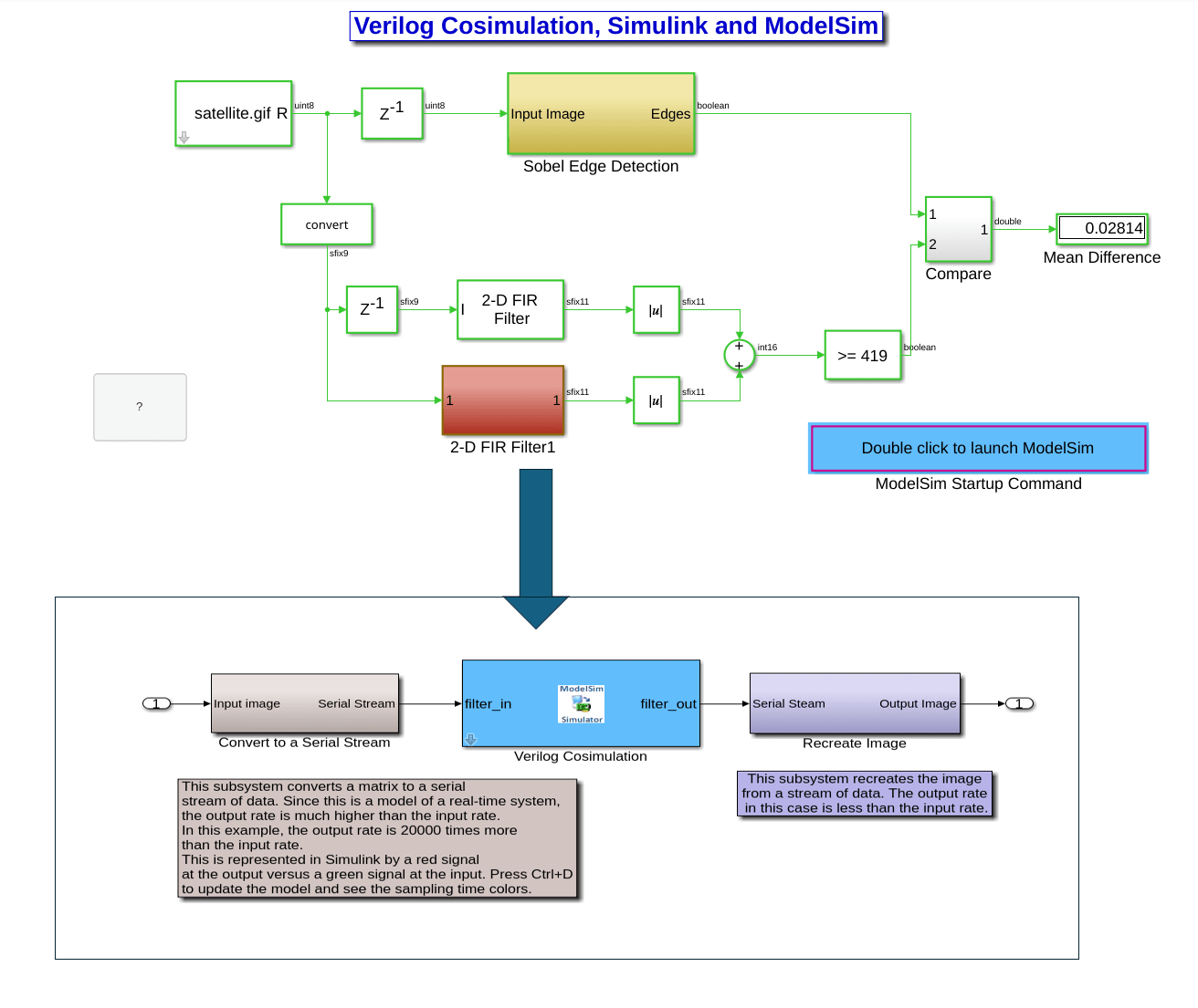
The model from the previous section can be passed to the HDL designer who can use the 2D filter designed in the last section to write the corresponding VHDL® or Verilog® code. Once the code is written, the HDL designer can use HDL Verifier™ to simulate the HDL design in the Simulink environment using ModelSim or Xcelium, and compare the output of the HDL design to the output of the executable specification. Note that in this process, there is no need for generating an HDL testbench. The Simulink model feeds the input test vector to ModelSim or Xcelium through HDL Verifier and extracts the data from ModelSim or Xcelium back to the Simulink environment. The HDL designer can readily verify whether the HDL code runs in accordance with the specifications.
ModelSim/QuestaSim
Refer to VHDL model or Verilog model to see how HDL Verifier is used to cosimulate Simulink and ModelSim. The last figure shows a snap shot of the signals displayed in ModelSim.
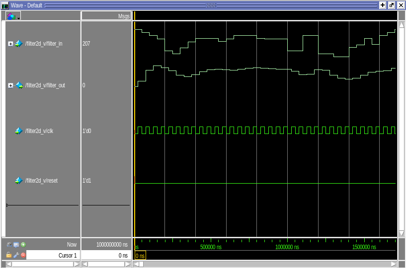
For Xcelium: Refer to Verilog model to see how HDL Verifier software is used to cosimulate Simulink and the Xcelium platform.