Generate HDL IP Core with AXI4 Master Interface to Access Altera External Memory
This example shows how to generate an HDL IP core that uses an AXI4 Master interface to interact with Altera® DDR4 external memory on the Intel® Arria® 10 SoC Development Kit. You perform read and write operations on the external memory using MATLAB® as the host.
Introduction
In this example, you:
Build a custom reference design by using Intel Platform Designer® and export the reference design to a Tcl script.
Add the exported Tcl script to the
plugin_rd.mfile in MATLAB®.Generate an HDL IP core with an AXI4 Master interface, create an Intel® Quartus® Pro project, build the bitstream, and program the target device.
Perform write and read operations to and from external memory using MATLAB as the host.
Verify the results in MATLAB® by comparing the data read back from the target with the expected values.
Requirements
To run this example, you need the following tools and hardware:
Intel® Quartus® Pro synthesis tool. For a list of supported versions, see HDL Language Support and Supported Third-Party Tools and Hardware.
Intel® Arria®10 SoC Development Kit.
HDL Coder™ Support Package for Intel FPGA and SoC devices.
HDL Verifier™ Support Package for Intel FPGA boards.
Design Architecture
This image shows the architecture of the design you use in this example.
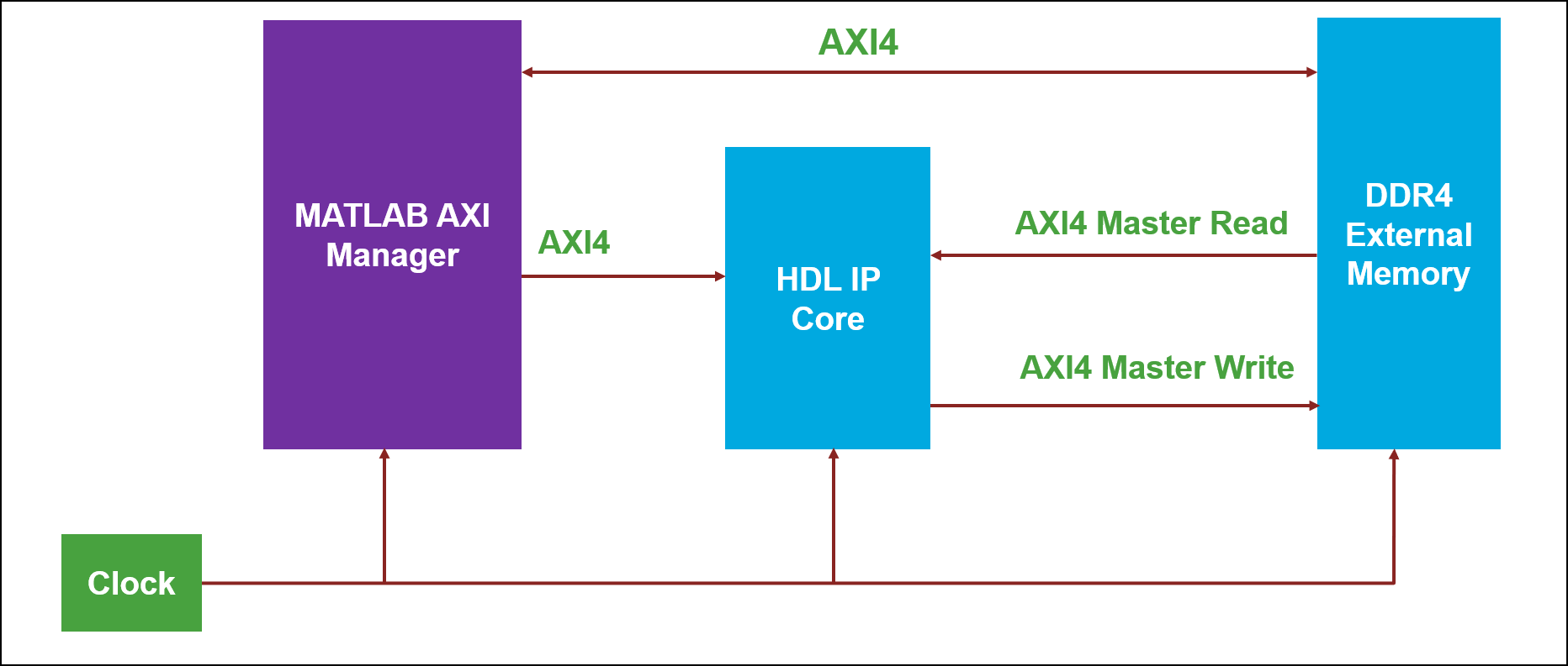
In this example, you generate an IP core from the DUT in the Simulink model. The IP core then connects to the HDL Verifier AXI Manager IP by using the AXI4 interface. The HDL Coder generates a DUT IP core that communicates with external DDR4 memory by using an AXI4 Master interface. The DUT also connects to the HDL Verifier AXI Manager IP by using the AXI4 interface. You can use the AXI Manager IP to:
Write raw input data to DDR4 memory.
Read processed output data for result verification.
During execution, the DUT reads input data from DDR4 memory by using the AXI4 Master Read interface. The DUT processes the data based on control signals and the DUT algorithm. After processing, the DUT writes the output data back to DDR4 memory using the AXI4 Master Write interface. MATLAB then reads the processed data from DDR4 memory by using the AXI Manager IP to validate the results.
Create Reference Design Using Intel Quartus Pro
To create and export the reference design, launch the Intel Quartus Pro synthesis tool and create a Quartus project that targets Intel Arria 10 SoC Development Kit. Use Platform Designer pane to construct a Qsys-based reference design.
You can use Platform Designer to create a sample reference design that includes these IP cores:
Clock Source IP
Intel IOPLL IP
External Memory Interface IP
By default, the design operates at a clock frequency of 50 MHz. However, you can configure this frequency based on your application requirements. The target frequency is determined by the output clock settings of the IOPLL IP, which directly drives the DUT IP core. Additionally, you can specify the clock frequency in the plugin_rd.m file.
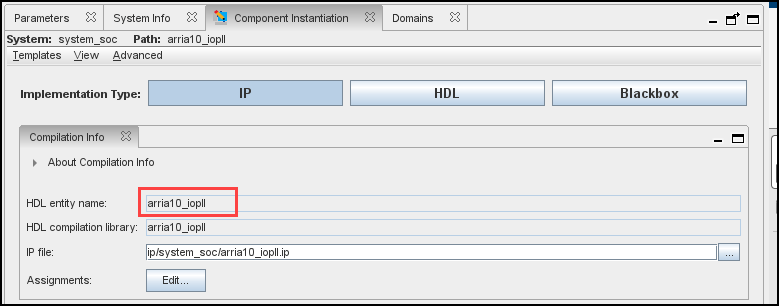
In Platform Designer, each IP core includes both an Instance name and HDL entity name. By default, Platform Designer prefixes the HDL entity name with system_soc, followed by the instance name. For example, if you set the instance name to iopll_0, the corresponding HDL entity name becomes system_soc_iopll_0.
If you want the HDL entity name to match the instance name exactly, set the HDL entity name when you add the IP to the reference design. After you add the IP, the HDL entity name is fixed and cannot be changed. However, you can modify the instance name at any time.
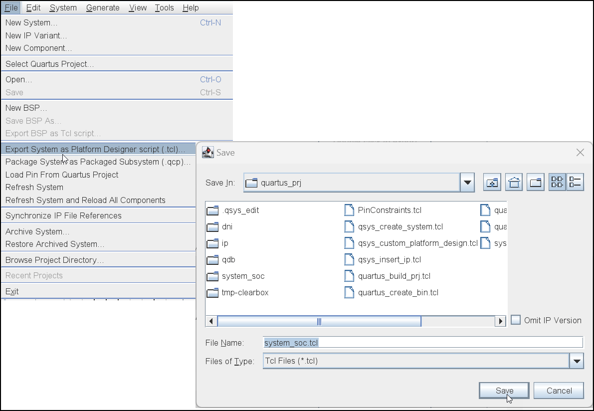
Export Reference Design to Tcl Script
After you construct the reference design, export the design to a Tcl script. At this stage, the HDL Coder generated DUT IP is not part of the reference design.
To export the design:
Open the completed Qsys system in Platform Designer.
Select File > Export System as Platform Designer Script.
Save the Tcl script to your project directory.
The Tcl script captures the structure and configuration of the reference design, including IP instances such as clock source, Intel IOPLL, and external memory interface.
Integrate Reference Design in plugin_rd.m
After you export the reference design to a Tcl script, register it in the plugin_rd.m file by using the hRD.addCustomQsysDesign API.
You can find the plugin_rd.m file at this location:
(matlabroot)/toolbox/hdlcoder/boards/intel/+IntelArria10SoC/+qpro_ddr_194
Make sure that the path and naming conventions match your board and reference design configuration.
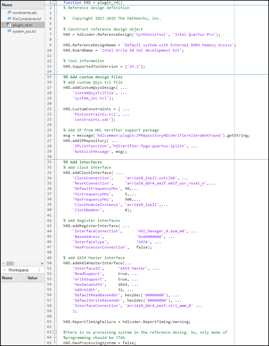
Define DUT Connections in plugin_rd.m
In the plugin_rd.m file, you explicitly define all connections to the DUT IP by using HDL Coder reference design registration APIs. Make these changes to match your design file:
Use the
hRD.addClockInterfaceAPI to specify the clock connection for the DUT. Set theClockConnectionparameter to indicate that the DUT IP clock connects to theoutclk0output of the Intel IOPLL IP.Define the clock frequency and supported frequency ranges in the same API call. These values represent the operating frequencies supported by the DUT IP. You can modify the default frequency to your desired target frequency directly in the
plugin_rd.mfile.Include the HDL Verifier AXI Manager IP in the reference design by using the
hRD.addIPRepositoryAPI. Use thehRD.addRegisterInterfaceAPI to establish the register-based communication path for data exchange and verification.
Note that, in the plugin_rd.m file, the ClockModuleInstance parameter is set to arria10_iopll. This name refers to the HDL entity name of the IOPLL IP, not the instance name.
Examine the Model and Design Under Test
To open the Simulink model, run these commands in the MATLAB Command Window:
modelname = "hdlcoder_external_memory";
open_system(modelname);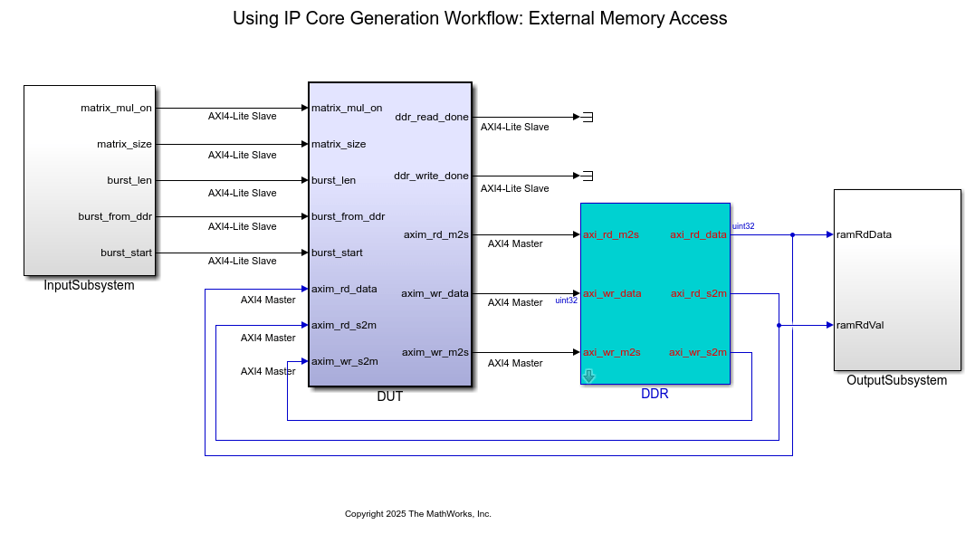
The model contains:
DUTsubsystem, which models the design under test (DUT).DDRsubsystem, which models the functional behavior of the DDR memory.InputSubsystemandOutputSubsystemsubsystems, which verify the model inputs and outputs.
The model implements a matrix-vector multiplication algorithm that targets the Intel Arria 10 SoC Development Kit. Because large matrices may not map efficiently to block RAMs on the FPGA fabric, the model stores the matrix data in external DDR4 memory on the FPGA board.
The DUT IP core accesses DDR4 memory by using the AXI4 Master interface, which communicates with vendor-provided memory interface IPs. The matrix-vector multiplication module supports fixed-point matrix arithmetic and a configurable matrix size ranging from 2 to 4000. You can configure the matrix size at runtime by using an AXI4-accessible register.
Open the DUT subsystem by running the following command in the MATLAB Command Window:
open_system("hdlcoder_external_memory/DUT");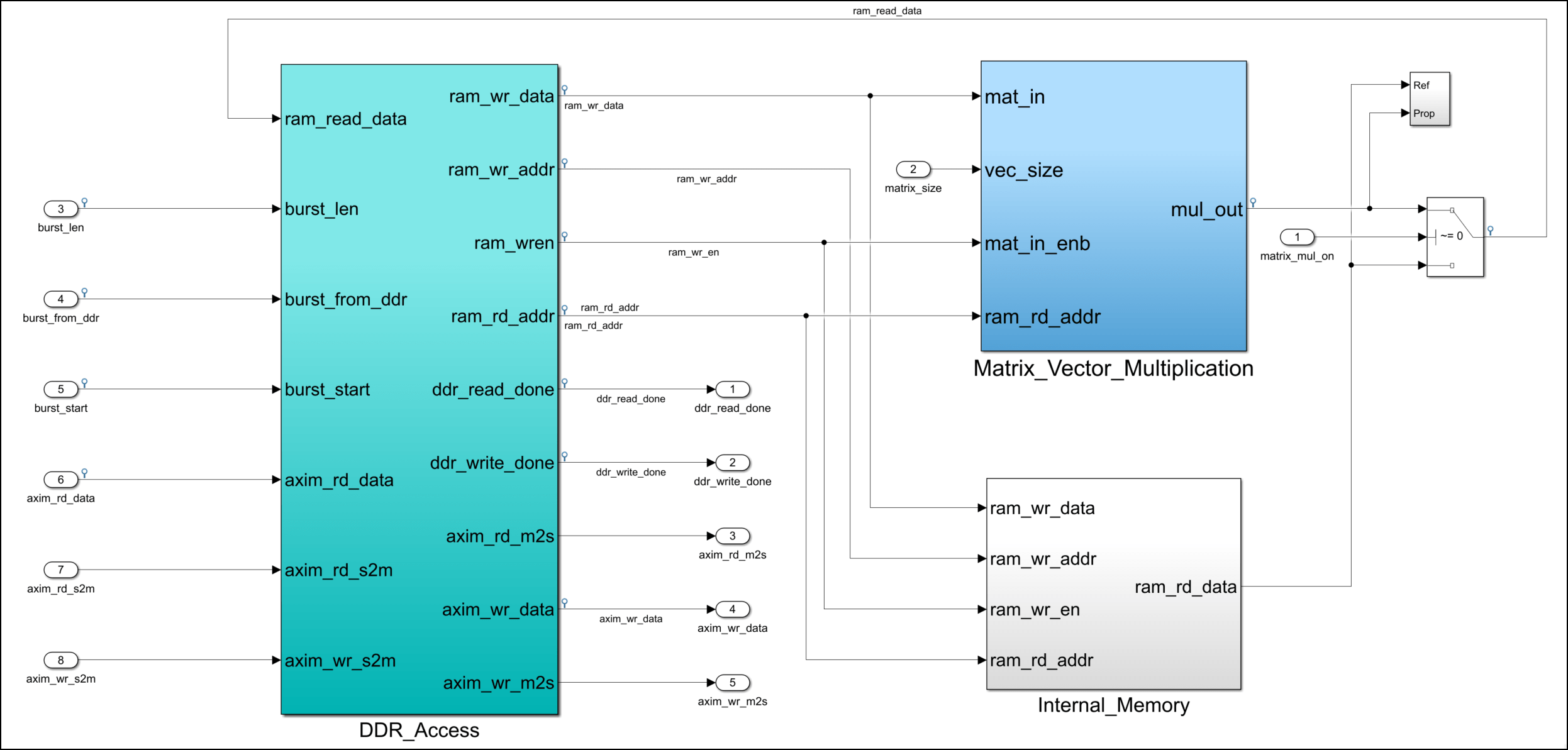
DUT Subsystem Overview
The DUT subsystem contains:
DDR_Acesssubsystem, which performs the AXI4 Master read and write controller operations.Matrix_Vector_Multiplicationsubsystem, which implements matrix-vector multiplication.Internal_Memorysubsystem.Parameter ports mapped to AXI4-accessible registers.
The DUT subsystem uses the AXI4 Master interface to read input data from external DDR memory, processes the data through the Matrix_Vector_Multiplication subsystem, and writes the output data back to DDR memory. You can use the Inport and Outport blocks to configure the design at run-time from MATLAB®, even after deployment to the FPGA.
You can control the DUT subsystem operation mode by using the matrix_mul_on Inport block.
When the signal from the
matrix_mul_onblock is true, theDUTsubsystem performs matrix-vector multiplication.When the signal from the
matrix_mul_onblock is false, theDUTsubsystem enters a data loop back mode. In this mode, the subsystem reads data from external DDR memory, writes it to theInternal_Memorysubsystem, and then write the same data back to the external DDR memory. You can use this mode to verify the functionality of the AXI4 Master-based external DDR memory access.
DDR_Access Subsystem
Within the DUT subsystem, the DDR_Access subsystem models a simplified AXI4 Master protocol for reading from and writing data to external DDR memory. During the IP core generation workflow, HDL Coder generates a translator that maps the simplified AXI4 Master protocol and the actual AXI4 Master protocol in the generated HDL IP core. For more information, see Model Design for AXI4 Master Interface Generation.
Matrix_Vector_Multiplication Subsystem
The Matrix_Vector_Multiplication subsystem uses a Multiply Add block to implement the streaming dot-product computation for matrix-vector multiplication. For more information, see Perform Large Matrix Operations Using External Memory.
Generate HDL IP Core with AXI4 Master Interface
Use the HDL Workflow Advisor to generate an IP core and deploy the design to the target device. For detailed instructions, see Get Started with IP Core Generation for Intel Quartus Pro Based Devices.
1. Set the path to your Intel Quartus Pro synthesis tool using this command in the MATLAB Command Window. Replace the path with your actual installation directory.
hdlsetuptoolpath("ToolName", "Intel Quartus Pro", "ToolPath", "C:\Altera\24.2_pro\Windows\quartus\bin64");
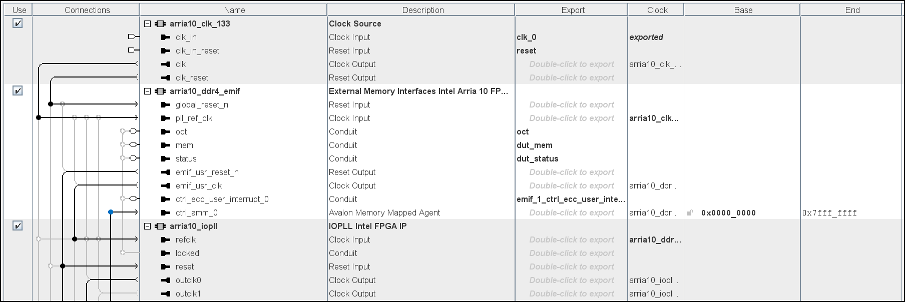
2. In the top model, select the DUT subsystem. On the HDL Code tab, click Workflow Advisor. In tasks 1.1 Set Target Device and Synthesis Tool, 1.2 Set Target Reference Design, and 1.3. Set Target Interface, set these parameters:
Target workflow:
IP Core GenerationTarget platform:
Intel Arria10 SoC development kitReference Design:
Default System with External DDR4 memory accessTarget platform interface table: Specify the settings in this image.
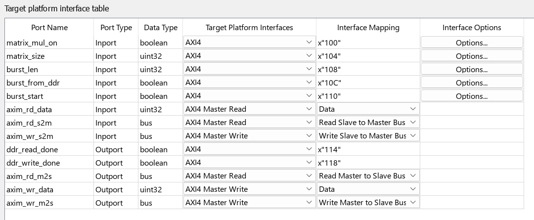
This example maps several input parameter ports to the AXI4-Lite interface, which enables you to configure them at run-time from MATLAB after deploying the design to the FPGA. HDL Coder generates AXI4-accessible registers for these ports. You can configure these ports in the Target platform interface table:
matrix_mul_on- Specifies whether the model uses matrix multiplication or loopback mode.matrix_size- Specifies the matrix dimension. This value must be an integer between 2 and 4000.burst_len- Specifies the burst length for AXI transactions.burst_from_ddr- Specifies the DDR read start address.burststart- Acts as a trigger signal for burst operation.
HDL Coder splits the AXI4 Master into read and write channels. You can also configure these channels in the Target platform interface table.
The read channel ports from the AXI4 Master Read interface are:
axim_rd_dataaxim_rd_s2maxim_rd_m2s
The write channel ports from the AXI4 Master Write interface are:
axim_wr_dataaxim_wr_s2maxim_wr_m2s
3. Right-click task 3.2. Generate RTL Code and IP Core and select Run to Selected Task. This step generates the IP core and associated files. After the task completes, you can view the register address mapping and related documentation in the generated IP Core Report.
4. Right-click task 4.2. Build FPGA Bitstream and select Run to Selected Task. This step creates the Intel Quartus Pro project, synthesizes the design, and builds the FPGA bitstream.
Integrate DUT IP and AXI Manager IP in Reference Design
During project creation, HDL Coder integrates the generated DUT IP core into the Default System with External DDR4 Memory Access reference design. HDL Coder also integrates the AXI Manager IP to enable MATLAB to:
Control the DUT IP.
Initialize DDR memory contents.
Verify results by reading back processed data.
Connect the s_axi interface of the DUT to:
ctrl_amm_0of the DDR IP (memory access)axm_m0of the AXI Manager IP (control from MATLAB)
This configuration enables the DUT to read the input data from DDR memory and receive control signals from MATLAB through the AXI Manager IP.
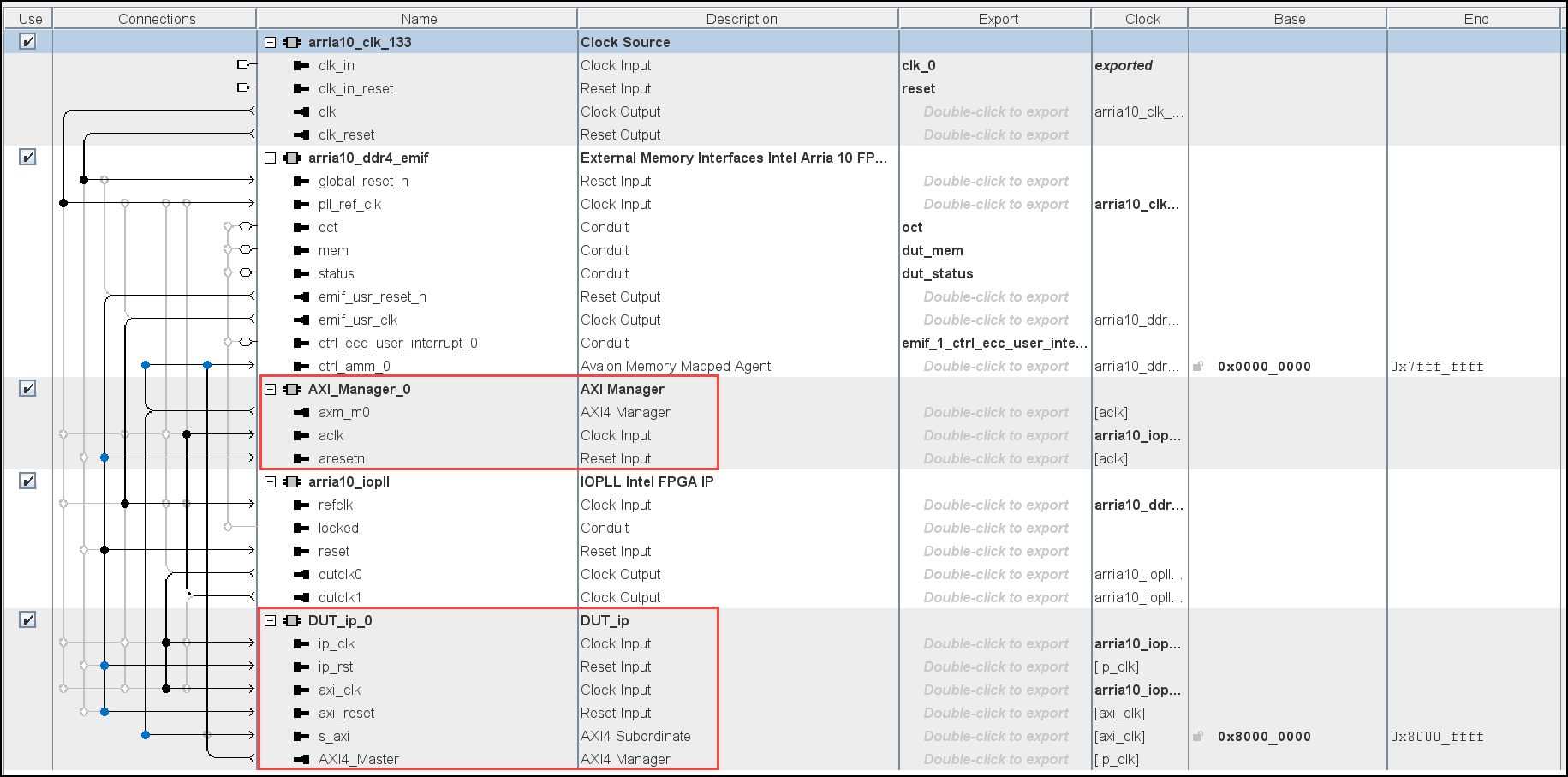
View Generated Quartus Project
To view the generated Intel Quartus Pro project after completing task 4.1.Create Project in HDL Workflow Advisor, click the link in the Result pane. In Quartus Pro, launch the Platform Designer. The reference design shows the project architecture, including the integrated DUT, DDR IP, and AXI Manager IP.
Perform Read and Write Operations and Verify Results Using MATLAB
After you generate the FPGA bitstream in the HDL Workflow Advisor, use task 4.3.Program Target Device to deploy the design to hardware. This step uses JTAG to load the bitstream onto the Intel Arria10 SoC Development Kit.
Verify Functionality Using MATLAB
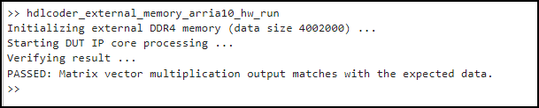
To verify the functionality of the deployed design on hardware, run this script in the MATLAB Command Window:
hdlcoder_external_memory_arria10_hw_run.m
This script performs a sequence of operations to verify the FPGA design on hardware by:
Initializing the parameters. The script sets
Matrix_Sizeto 500, which indicates a 500 x 500 matrix. You can configure this value up to 4000.Configuring the AXI Master base addresses. The script sets the read base address to
00000000and the write base address to10000000. These addresses define where the DUT reads from and writes to in external DDR memory.Initializing the DDR memory. Using the AXI Manager, the script writes input vector and matrix data to DDR memory and clears the output memory region by using
writememory.Starting the DUT. The script uses the AXI4-accessible registers to start the
DUT. TheDUTreads input data from DDR, perform matrix-vector multiplication, and write the results back to DDR memory.Reading and verifying output. The script reads the output data from DDR memory by using
readmemoryand compares the results with the expected values in MATLAB.
The script generates this output: