Generate Clock-Domain-Crossing Pulse Synchronizer by Generating a Multiple-Clock IP Core
In field programmable gate array (FPGA) and application-specific integrated circuit (ASIC) designs, different modules often operate in separate asynchronous clock domains. Transferring data between these domains without synchronization can result in data corruption due to metastability. To mitigate the effects of metastability, you must transfer data between asynchronous clock domains by using clock domain crossing (CDC) synchronization logic.
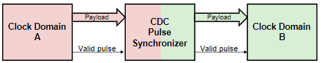
This image shows a common pattern for transferring multi-bit data between two asynchronous clock domains that have a known relationship. The valid data pulse that accompanies the data payload that originates in clock domain A indicates when new data is available. The CDC pulse synchronizer then transfers the payload to clock domain B.
This example shows how to:
Model and simulate a CDC pulse synchronizer in Simulink®.
Generate a multiple-clock HDL IP core using HDL Coder™.
Integrate the multiple-clock IP core into an AMD Vivado™ project.
Use host interface scripts to test the design on hardware.
To interact with the deployed IP core, you must:
Install HDL Coder™ Support Package for AMD FPGA and SoC Devices
Download the MathWorks® firmware image on the ZedBoard SD card. For help with SD card setup, see Guided Hardware Setup for AMD Boards.
System Overview
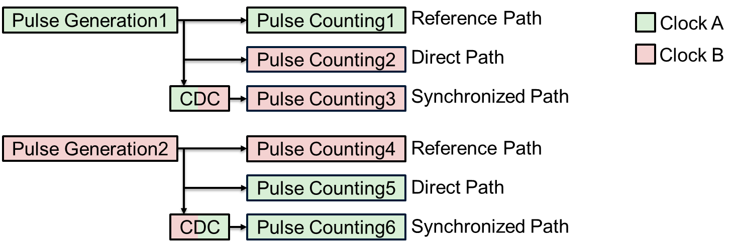
In this example, the design includes two pulse generators, one in the slow clock domain (clock A) and one in the fast clock domain (clock B). This image shows the three parallel data paths for both pulse generators. In the reference path, the pulse counting logic counts the pulses in the originating clock domain. In the direct path, the pulse generator sends pulses directly to the destination clock domain and counts the pulses without CDC synchronization. If the destination clock runs faster than the originating clock, it may count some pulses more than once. If the destination clock runs slower, it may miss pulses. In the synchronized path, the pulses pass through a CDC pulse synchronizer before the destination clock counts the pulses, which ensures that the count matches the reference path.
 I
I
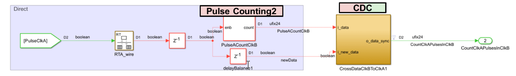
To store the counts in AXI4-Lite registers, which reside in clock domain A, the design synchronizes the output of the pulse counters from clock domain B with clock domain A. This image shows how the design uses a CDC pulse synchronizer to synchronize the multi-bit count data to the clock A domain. The counter value is the data payload, and the pulse acts as a valid signal that indicates when to sample or transfer the data.

Open and Examine the Model
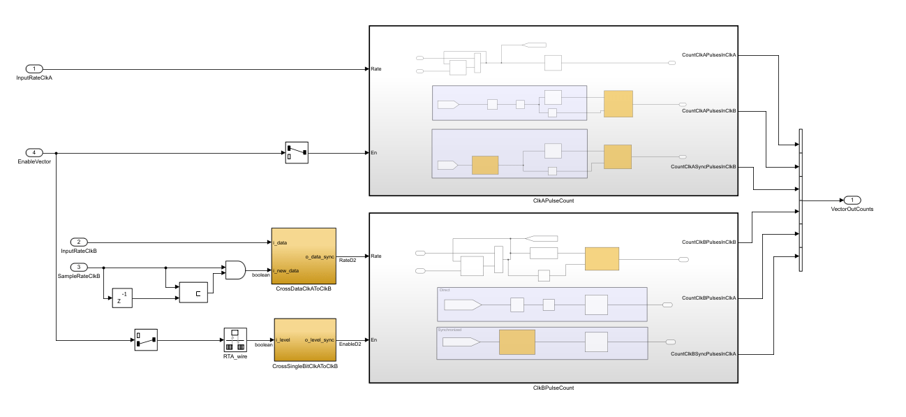
In the hdlMultiClockCounts model, the device under test (DUT) contains two subsystems, ClkAPulseCount and ClkBPulseCount, that implement the pulse generators and pulse counting logic for each clock domain. The ClkAPulseCount subsystem represents the slow clock domain, clock A, and ClkBPulseCount represents the fast clock domain, clock B.
load_system("hdlMultiClockCounts");
open_system("hdlMultiClockCounts/DUT");
Clock A uses a frequency of 50 MHz and the sample time Ts, and clock B has a frequency of 141.39785 MHz and a sample time of Ts2. The model uses the InitFcn callback function to set the sample times for both subsystems. To view and edit the InitFcn callback function, right-click in the Simulink canvas, click the Model Properties ![]() button, select the Callbacks tab, and then click InitFcn in the left pane.
button, select the Callbacks tab, and then click InitFcn in the left pane.
Open the ClkAPulseCount subsystem to see the three parallel data paths for the pulse generator in the clock A domain.
open_system("hdlMultiClockCounts/DUT/ClkAPulseCount");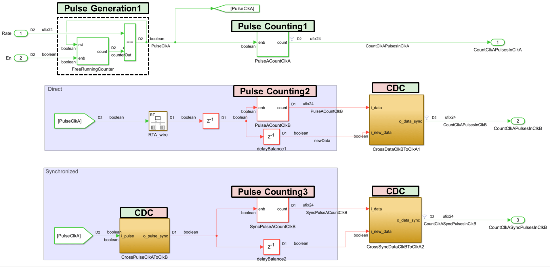
The ClkAPulseCount subsystem contains implementation of the:
Reference path, which counts pulses in the clock A domain.
Direct path, which generates pulses and counts them in the clock B domain without synchronization.
Synchronized path, which generates pulses and counts them in the clock B domain by using a CDC-based pulse synchronizer.
Reference Path
To generate the pulse, the model uses a free-running counter. When the counter reaches the value specified by the Rate Inport block, it generates a pulse signal, PulseClkA. The HDL Counter block PulseACountClkA uses these pulses as the enable signal to count the periodic pulses in the originating clock domain.
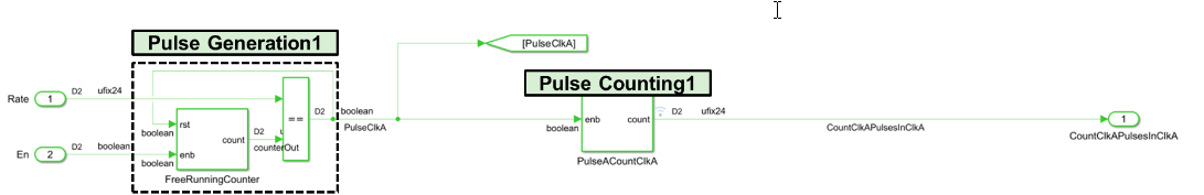
Direct Path
The reference path output PulseClkA connects to a Delay block through a Rate Transition block, RTA_Wire. The output of the Delay block connects to the PulseACountClkB block, which counts the clock A pulses in clock B without CDC synchronization. To observe the missed pulse counts during implementation, the customDUTCDC XDC file contains attributes to mark the direct path as a false path or omit the path.
The output of the PulseACountClkB block connects to the CrossDataClkBToClkA1 block, which synchronizes all count data from clock domain B back to clock domain A.
To store all counts in the same clock domain, the design synchronizes all count data from clock domain B back to clock domain A. A common method for transferring data between different clock domains is to use a dual-clock first-in first-out (FIFO) buffer. If the data transfer rate is low and you need only a single-bit signal to indicate data availability, a pulse CDC synchronizer can be a more resource-efficient alternative. Also, this approach is independent of FPGA technology.
To view the implementation, open the CrossDataClkBToClkA1 block in the ClkAPulseCount subsystem.
open_system("hdlMultiClockCounts/DUT/ClkAPulseCount/CrossDataClkBToClkA1");
The input pulse i_new_data latches the multi-bit data count i_data in the originating clock domain. The design uses a pulse synchronizer to synchronize the input pulse to the destination clock domain. You cannot trigger new data while the i_new_data pulse propagates.
Synchronized Path
The model synchronizes the pulse in the blocks in the Synchronized area by using a pulse synchronizer implemented in the CrossPulseClkAToClkB subsystem. The output signal enables the HDL Counter block SyncPulseACountClkB , which uses the destination clock domain, clock domain B.
Pulse Synchronization
To view the pulse synchronizer, open the CrossPulseClkAToClkB subsystem.
open_system("hdlMultiClockCounts/DUT/ClkAPulseCount/CrossPulseClkAToClkB");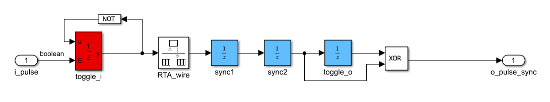
This subsystem can convert signals from fast-to-slow and slow-to-fast clock domains when the input pulses in the originating clock domain are at least two destination clock periods apart.
The Inport block Rate in the ClkAPulseCount subsystem determines the spacing between pulses in the originating clock domain for the pulse synchronizers in the ClkAPulseCount subsystem. The ClkAPulseCount subsystem generates a pulse for every Rate + 1 of the originating clock cycles. To determine the minimum safe value for the CrossPulseClkAToClkB subsystem, use this formula:
Rate > 2* (originating clock frequency/ destination clock frequency)
In CrossPulseClkAToClkB, the originating clock is 50 MHz and the destination clock is 141.39785 MHz, so, the signal from the Rate block must be greater than 2*(50/141.39785), that is, Rate greater than 0.73. Because Rate must be an integer greater or equal to one, round up to the next whole number. In practice, you may choose a larger value to ensure robust operation. For the ClkAPulseCount subsystem, the signal from the Rate block is set to 2e12.
The output of the toggle_i Unit Delay Enabled Synchronous block toggles from high to low and then low to high every time an input pulse arrives from the i_pulse Inport block. The output of the toggle_i block is a level signal that the subsystem can synchronize to the destination clock domain by using two flip-flop synchronizers, represented by the sync1 and sync2 Unit Delay blocks. The sync2 block has two output signals, one that connects directly to the XOR block, and one that connects to the XOR block after being delayed one clock cycle by the toggle_o Unit Delay block.
Because the example in this model explicitly synchronizes the clock domains, the clock domain transitions must be wires in the register-transfer level (RTL). To represent this, the CrossPulseClkAToClkB subsystem uses the Rate Transition Block, RTA_wire with the Ensure data integrity during data transfer and Ensure deterministic data transfer block parameters cleared, and the AsyncRTAsWire HDL Block property set to true. The Output port sample time of the Rate Transition block is the destination clock sample time, Ts2.
To set these settings, at the MATLAB command line, enter:
hdlset_param("hdlMultiClockCounts/DUT/ClkAPulseCount/CrossPulseClkAToClkB/RTA_wire","AsyncRTAsWire","on");
set_param("hdlMultiClockCounts/DUT/ClkAPulseCount/CrossPulseClkAToClkB/RTA_wire", "Integrity", "off");
set_param("hdlMultiClockCounts/DUT/ClkAPulseCount/CrossPulseClkAToClkB/RTA_wire","Deterministic","off");
set_param("hdlMultiClockCounts/DUT/ClkAPulseCount/CrossPulseClkAToClkB/RTA_wire","OutPortSampleTime","Ts2");
Timing Constraints and Synthesis Attributes
Synthesis tools require specific directives for timing analysis of multi-clock paths. You can set some directives directly in the HDL code using synthesis attributes. You must use timing constraints to specify timing exceptions. To apply the necessary timing constraints, define custom synthesis attributes in your HDL code that mark signals of interest and then reference them in Tcl scripts.
The generated code for synthesis attributes depends on synthesis tool. This example uses AMD Vivado to deploy the generated code to the ZedBoard™. The attributes in this example are specific to AMD Vivado. If you use a different tool, you must set the tool specific synthesis attributes specific to your tool.
For the pulse synchronizer in CrossPulseClkAToClkB:
To place the two registers of the level synchronizer,
sync1andsync2together during synthesis and implementation,the ASYNC_REG synthesis attribute is set to true. The ASYNC_REG attribute tells Vivado that a register is used for synchronizing asynchronous signals and places directly connected flip-flops together.The path from the originating clock domain to the first flip-flop of the synchronizer is a false path. To specify this path as a timing exception, the custom synthesis attribute cdc_falsepath is set to data on the same signal to later identify it in the timing constraint. In this synchronizer, ASYNC_REG preserves the signal at the output of the
sync1delay block. For more information on how to set synthesis attributes, see Configure Custom Synthesis Attributes for Simulink Blocks.
To see the synthesis attributes for the CrossPulseClkAToClkB subsystem, at the MATLAB command line, enter:
hdlget_param("hdlMultiClockCounts/DUT/ClkAPulseCount/CrossPulseClkAToClkB/sync1","SynthesisAttributes");
hdlget_param("hdlMultiClockCounts/DUT/ClkAPulseCount/CrossPulseClkAToClkB/sync2","SynthesisAttributes");
The customDUTCDC.xdc file contains these Tcl commands to set the false path during synthesis:
set falsepathregcells [get_cells -hier -filter {cdc_falsepath=="data"}]
set falsepathregpins [get_pins -of_objects $falsepathregcells -filter {REF_PIN_NAME=="D"}]
set_false_path -to $falsepathregpins
Clock B to Clock A Pulse Transfers
The DUT subsystem includes a second subsystem, ClkBPulseCount, which has the same structure as the ClkAPulseCount subsystem. Open the ClkBPulseCount subsystem to inspect the pulse generation and counting. This subsystem:
Synchronizes the counts to the slower clock domain, clock A.
Includes blocks in each subsystem with the necessary synthesis attributes for manual timing constraints.
open_system("hdlMultiClockCounts/DUT/ClkBPulseCount");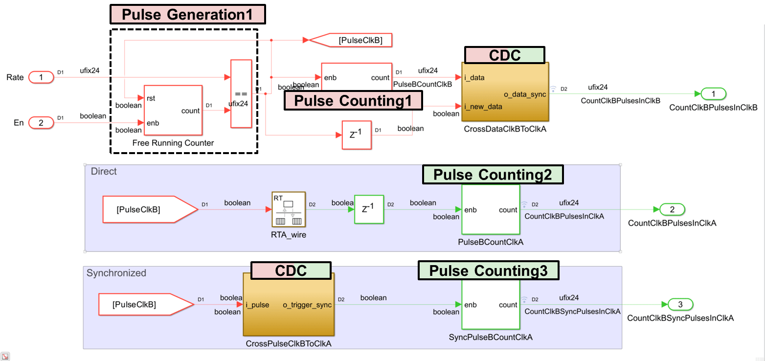
Timing Constraints and Synthesis Attributes
Open the CrossDataClkAToClkB subsystem.
open_system("hdlMultiClockCounts/DUT/CrossDataClkAToClkB")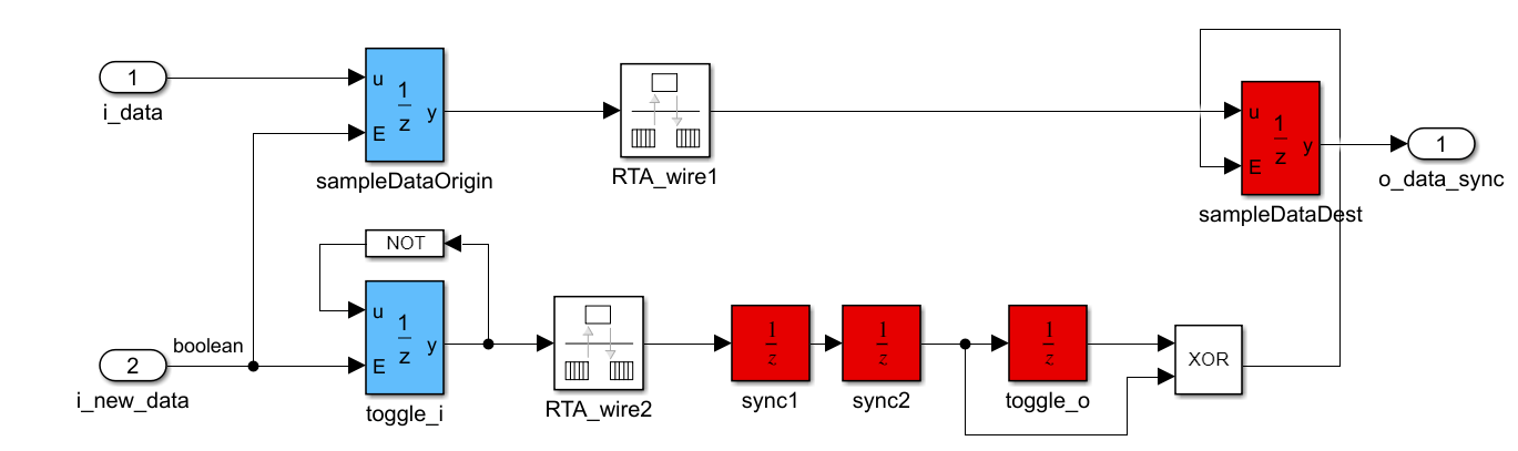
Because the pulse synchronization takes at least two destination clock periods, so the sampleDataDest register in general is stable after two clock periods. To tighten the requirement, you must set a max_data_path_delay constraint in this data path that is equal to one clock period of the destination clock domain. To set the max_data_path_delay constraint, set these custom synthesis attributes:
cdc_maxpathtodata_clkBtoclkA_starton the output signal of thesampleDataOriginregistercdc_maxpathtodata_clkBtoclkA_endon thesampleDataDestregister output signalcdc_maxpathtoclk_clkBtoclkAon the output signal of a register in the synchronizer such astoggle_o
To use the custom synthesis attributes to set the max_data_path_delay constraint during synthesis, the customDUTCDC XDC file includes these Tcl commands:
set reg_clkBtoclkA [get_cells -hier -filter {cdc_maxpath=="clk_clkBtoclkA"}]
set clk_clkBtoclkA [get_clocks -of $reg_clkBtoclkA]
set clk_period_clkBtoclkA [get_property PERIOD $clk_clkBtoclkA]
set startreglist_clkBtoclkA [get_cells -hier -filter {cdc_maxpath=="data_clkBtoclkA_start"}]
set endreglist_clkBtoclkA [get_cells -hier -filter {cdc_maxpath=="data_clkBtoclkA_end"}]
set_max_delay -from $startreglist_clkBtoclkA -to $endreglist_clkBtoclkA -datapath_only $clk_period_clkBtoclkA -quiet
To synchronize the enable signal of the clkBPulseCount pulse generator, use a two flip-flop synchronizer to represent a binary level signal. The CrossSingleBitClkAToClkB subsystem implements this synchronizer, including the necessary synthesis attributes for the necessary timing constraints.
To synchronize the InputRateClkB Inport block value, the block uses an additional Boolean signal to indicate when the rate is valid for reading. When this input changes from 0 to 1, the synchronizer generates a pulse to indicate the input rate is ready for transfer, and transfer the data using a pulse synchronizer. Open the CrossDataClkAToClkB subsystem to view the CDC synchronizer:
open_system("hdlMultiClockCounts/DUT/CrossDataClkAToClkB");
Simulate the Model
Next, simulate the model to verify the functional behavior of the pulse synchronizer and observe how it transfers pulses across clock domains. While behavioral simulation cannot model metastability, it can help verify pulse synchronizer operation.
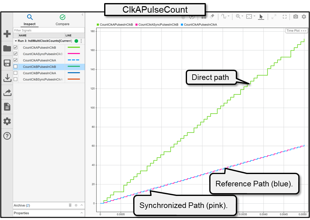
This model uses the variable step discrete solver to simulate the behavior of the synchronization logic. Simulate the model. After the simulation completes, open the Simulation Data Inspector by clicking Data Inspector on the Simulation tab.
To see the behavior of each subsystem:
For
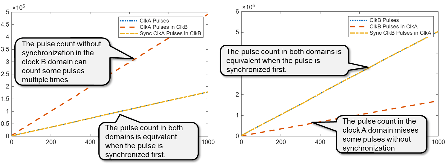
ClkAPulseCount: In the Simulation Data Inspector, select the CountClkAPulsesInClkB, CountClkASyncPulsesInClkB, and CountClkAPulsesInClkA signals. The simulation shows that the reference path count, CountClkAPulsesInClkA matches the synchronized path count, CountClkASyncPulsesInClkB. The direct path, CountClkAPulsesInClkB demonstrates that the counter counts some pulses multiple times because the originating clock domain is slower than the destination clock domain.
For
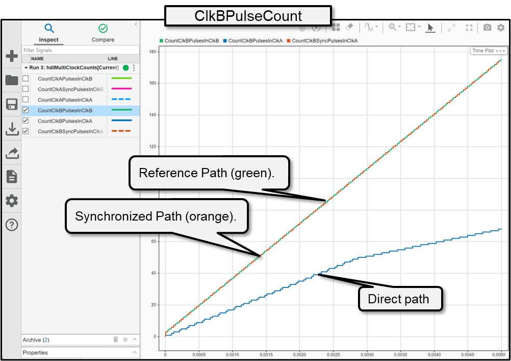
ClkBPulseCount: Select the CountClkBPulsesInClkA, CountClkBSyncPulsesInClkA, and CountClkBPulsesInClkB signals. The simulation shows that the reference path count, CountClkBPulsesInClkB matches the synchronized path count, CountClkBSyncPulsesInClkA. The direct path, CountClkBPulsesInClkA demonstrates that the counter misses some pulses because the originating clock domain is faster than the destination clock domain.
Generate Multiple-Clock IP Core
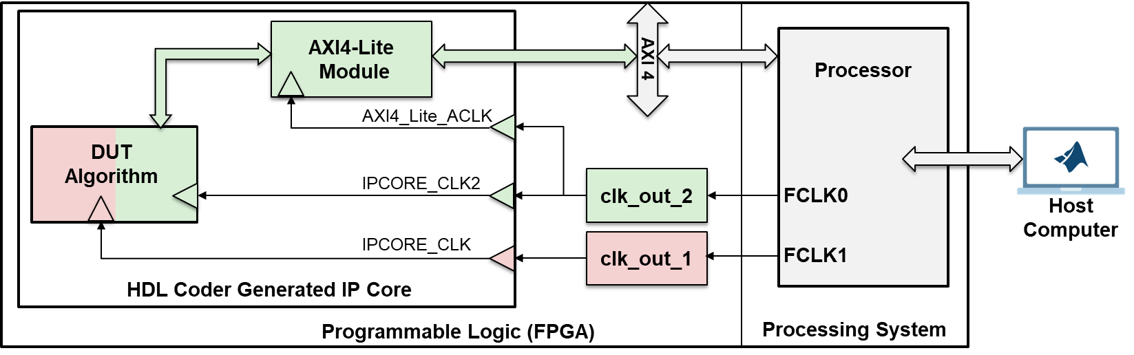
In multiple-clock mode, HDL Coder generates a clock input port for each Simulink rate in the design under test (DUT). This high-level architecture diagram illustrates the system in this example. The generated IP core includes two clock inputs, each mapped to the corresponding clock domains in the DUT. The AXI4-Lite interface module has its own clock port, which connects to the slower clock domain, clock A. The host computer can tune parameters by writing to AXI4-Lite registers in the IP core, and can read data back from the IP core to verify that synchronized path count values match the reference count value in each clock domain.
When generating an HDL IP core, you only need to model the data ports. HDL Coder inserts logic to connect the DUT to AXI4 or AXI4-Lite interface buses and creates the required AXI-accessible registers. If the DUT has vector ports, HDL Coder synchronizes data transfers using strobe and shadow registers. To sample all counts simultaneously, the design concatenates the output counts from each subsystem into a single vector, VectorOutCounts and maps it to an AXI4-Lite register. Similarly, the EnableVector input is a logic vector that supplies the enable signal for each subsystem, which enables both subsystem enable inputs to toggle at the same time. Independent registers control the input rates for both subsystems. To view the input and output mapping for the DUT, open the DUT subsystem block.
open_system("hdlMultiClockCounts/DUT");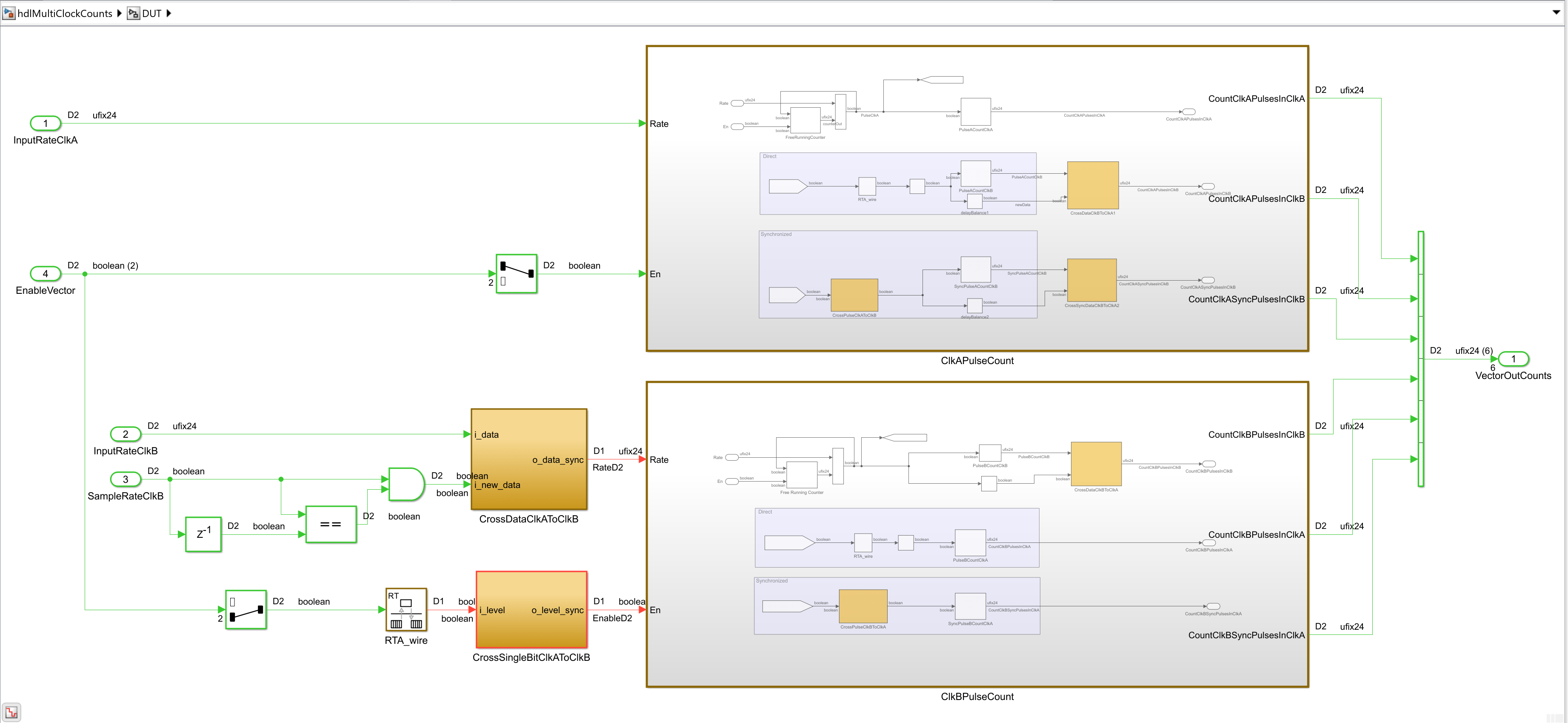
In this example, the AXI4-Lite interface uses a single clock, and the inputs and outputs of the DUT must operate at the same rate. The ClkAPulseCount subsystem inputs have the same rate as the AXI4-Lite interface and the inputs of the ClkBPulseCount subsystem operate at a different rate.
To configure the model for IP core generation:
1.Set up the Xilinx Vivado synthesis tool path, by using the hdlsetuptoolpath function. Use your own Vivado installation path when you run the command.
hdlsetuptoolpath("ToolName","Xilinx Vivado","ToolPath",vivadopath)
2. In the Apps tab, click HDL Coder. In the HDL Code tab, in the Output section, set the drop-down button to IP Core. In the Generate Code section, set Code for to DUT.
3. Click Settings to open the HDL Code Generation > Target pane of the Configuration Parameters dialog box.
4. Set Target Platform to Generic Xilinx Platform and set Synthesis Tool to Xilinx Vivado.
5. In the left pane, click HDL Code Generation > Global Settings. Set Clock inputs to Multiple.
Configure Design and Target Interface
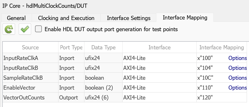
Next, configure the design to map to the target hardware by mapping the DUT ports to the IP core target hardware and setting the DUT-level IP core options. In this example, map all DUT ports to AXI4-Lite interfaces.
In the IP Core pane, select the Interface Mapping tab. If the mapping table does not appear, click the Reload IP core settings button
 to compile the model and populate the DUT ports and their data types.
Validate your settings by clicking the Validate IP core settings button
 .
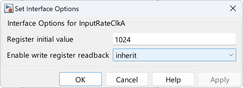
.Click the Options link next to
InputClkRateAandInputClkRateBand in the Set Interface Options dialog box, set Register initial value to a non-zero value. This setting ensures the pulse generators are idle at reset and only start when enabled.
Next, generate the IP core. In the Simulink Toolstrip, in the HDL Code tab, click Generate IP Core.
After the software generates the IP core, it opens the IP core report, which contains details of the multiple clock connections, behavior, and contents of the generated custom IP core.
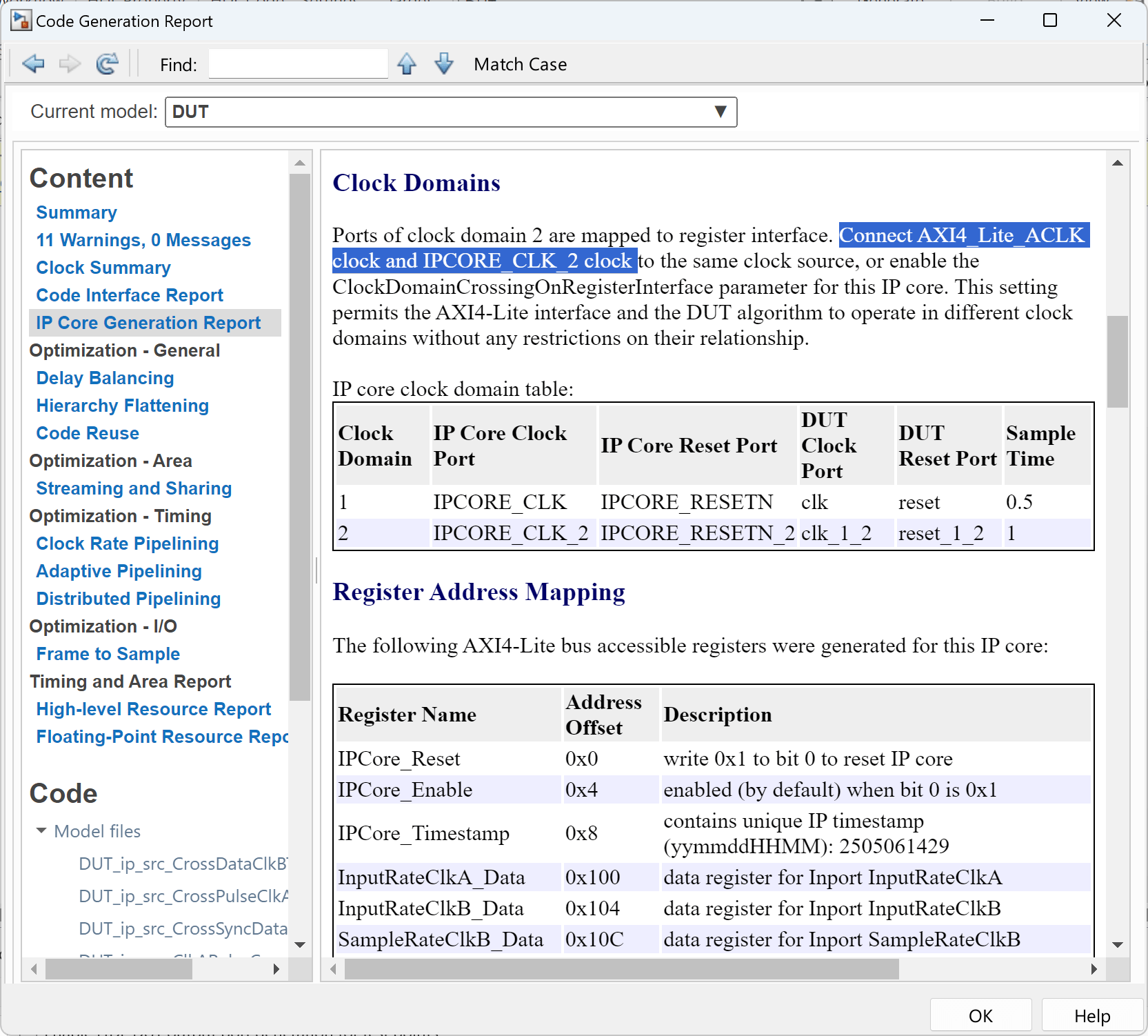
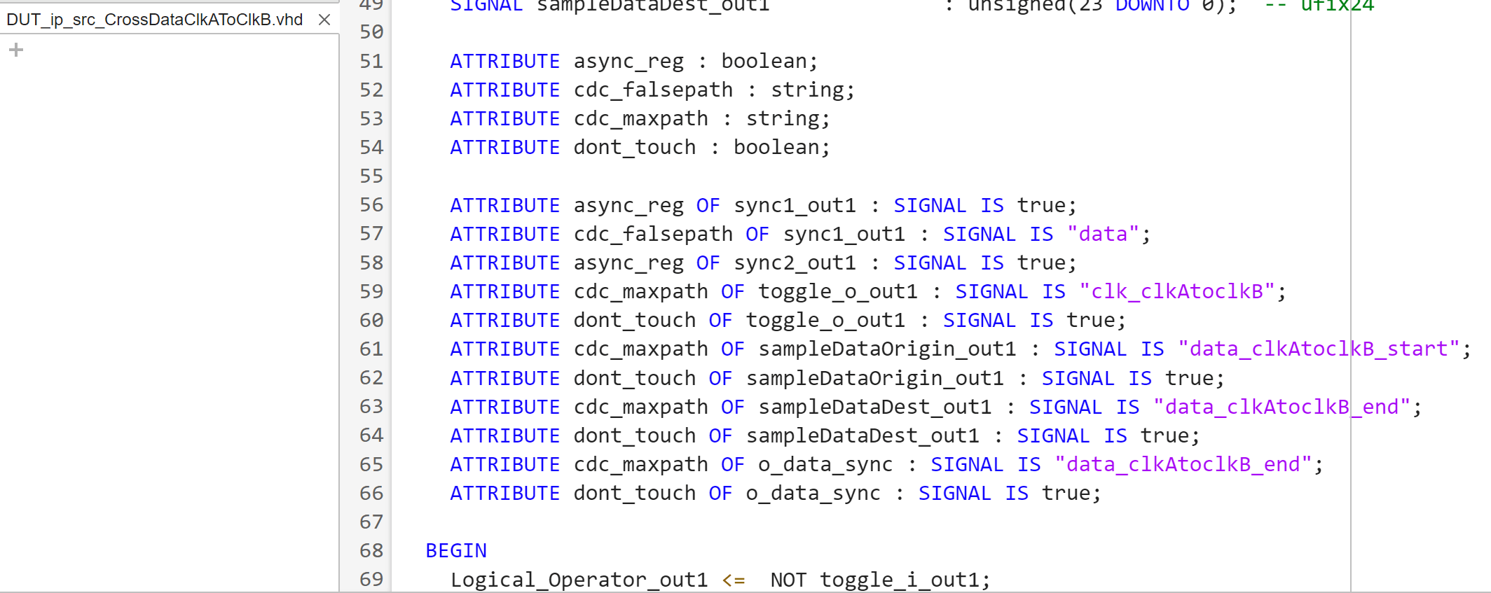
To view the synthesis attributes that HDL Coder added to the CDC synchronization logic, inspect the generated HDL code for one of the synchronizers. For example, this image shows the contents of the DUT_ip_src_CrossDataClkAToClkB.vhd file.
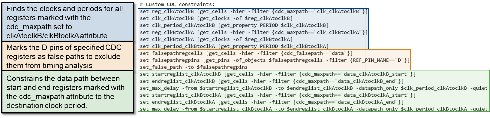
Based on the custom synthesis attributes, to constrain your design, the customDUTCDC XDC file includes a custom set of Tcl commands. This image shows the contents of the customDUTCDC.xdc file and a description of the actions performed by the commands.
To add these constraints to the packaged HDL IP core:
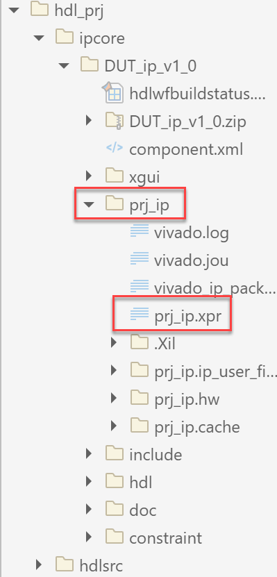
1. Navigate to the location of the packaged IP core project, prj.xpr. To open the XPR file in Vivado, at the MATLAB command line, enter:
!vivado prj_ip.xpr &
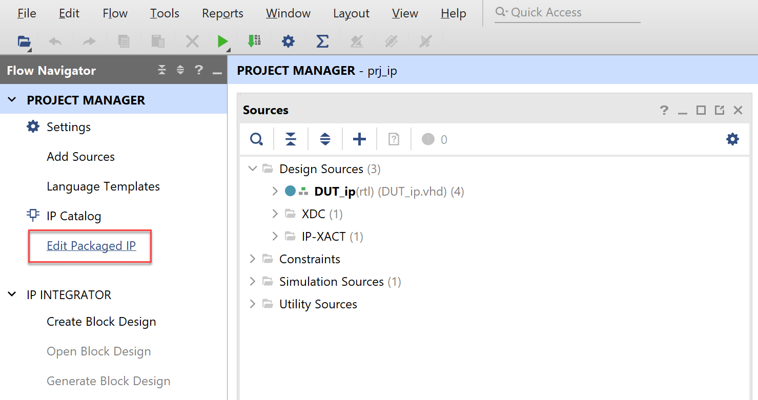
2. In Vivado, click Edit Packaged IP to open the IP Packager.
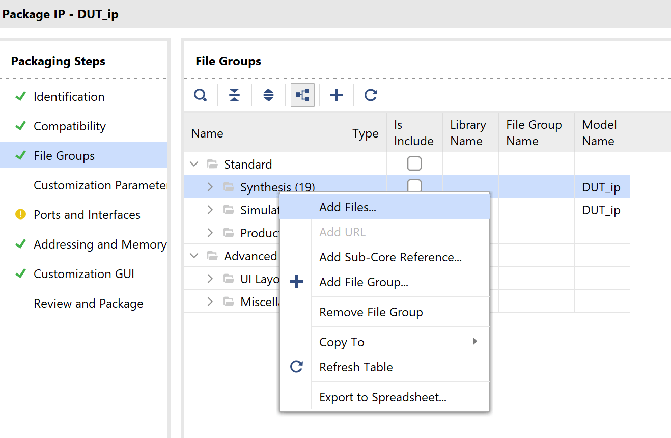
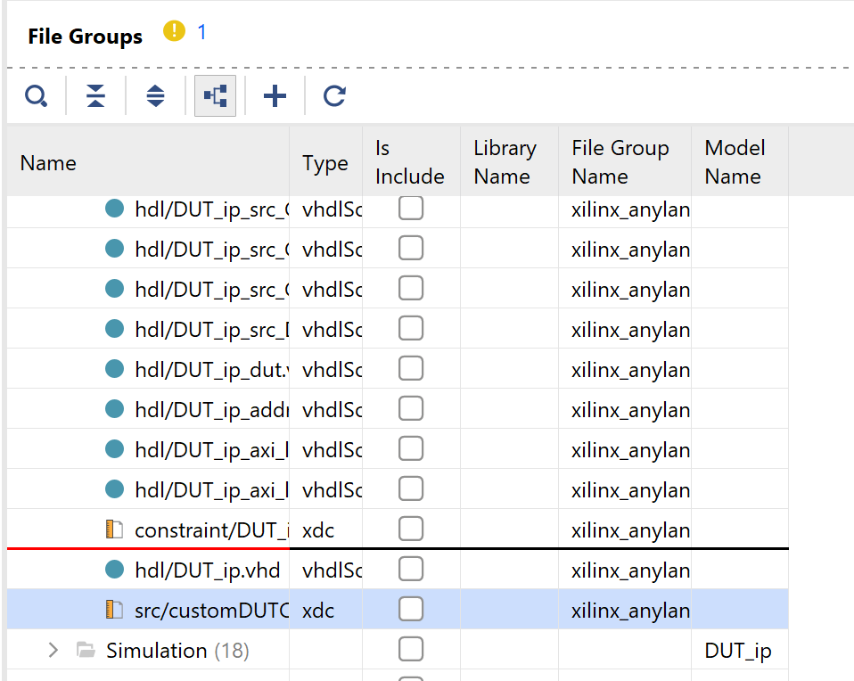
3. Click File Groups to see the design sources in the IP core. Vivado displays design sources, including the autogenerated timing constraint file DUT_ip_hdlc_CDC_constraint.xdc for the multi-clock IP core. HDL Coder generates the constraints during IP core generation including constraints that synchronize the DUT enables and IP core resets in each clock domain. To add the custom constraint for the logic in the DUT, in the File Groups pane, right click Synthesis and then click Add Files.
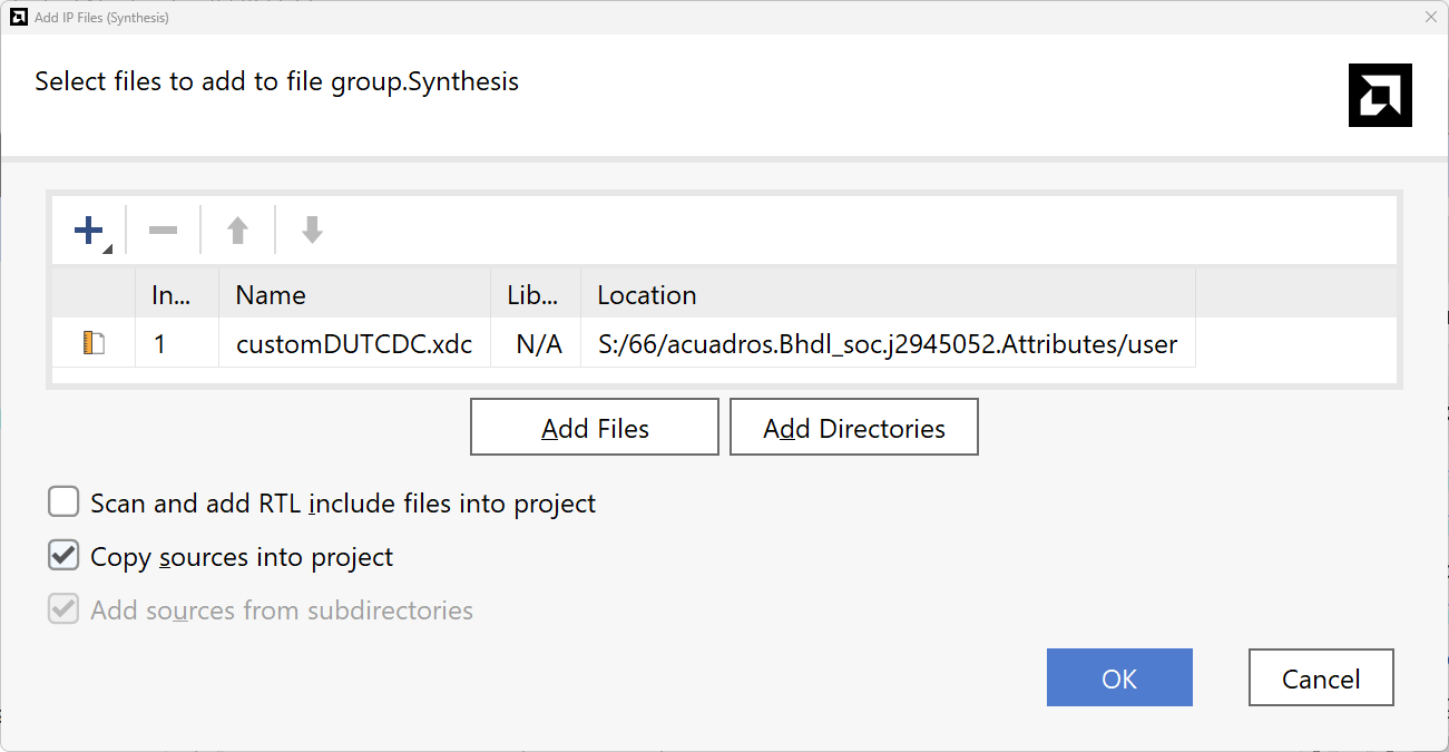
4. Select the XDC constraints file and enable Copy sources into project.
5. If you get a warning message to verify that a HDL code file is the last file in the list, move the XDC file before the last HDL code file, as shown in this image.
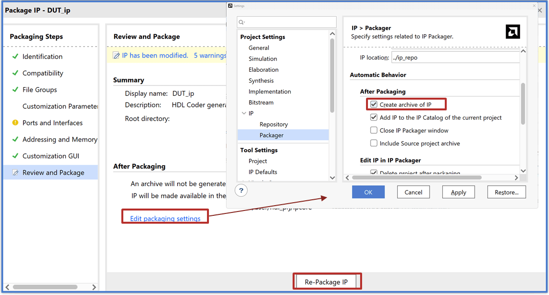
6. In Review and Package, click Re-Package IP. Optionally, to generate an archive of the IP core, click Edit packaging settings, and enable the Create archive of IP.
Insert HDL IP Core in Xilinx Vivado SoC Project
To use the generic IP core as part of a larger system, create a Vivado project, integrate the multi-clock IP core, and generate a bitstream for your target platform.
1. To create a project, you can use the create_custom_prj.tcl file in Vivado. This Tcl file contains commands that creates a new directory for the project, configures the project to target a ZedBoard, and uses a pre-created block design containing the processor, interconnects, and clock wizards to test the IP core. To open Vivado and execute the TCL command, at the MATLAB command line, enter:
!vivado -source create_custom_prj.tcl &
2. Use these Tcl commands to add the generated HDL Coder IP core to the IP catalog. Replace the file path with the path to your XPR project file.
open_project C:/Users/user/CDCExample/hdl_cdc/hdl_cdc.xpr
set_property  ip_repo_paths  C:/Users/user/CDCExample/hdl_prj/ipcore/DUT_ip_v1_0 [current_project]
update_ip_catalog
For additional information on how to insert a custom IP core generated with HDL Coder into an AMD Vivado project, see Generate Board-Independent HDL IP Core for Xilinx Platforms.
3. Integrate the IP Core:
Open the block diagram. In the Project manager pane, click Open block diagram.
In the block diagram, insert the generated IP. To insert the IP generated by HDL Coder, right-click inside the block diagram and select Add IP. Search for the name of the IP and press Enter.
The example targets a ZedBoard with two PLL clocks:
FCLK_CLK0at 100 MHz andFCLK_CLK1at 200 MHz, each of which feeds a clock wizard that generates the required frequencies. For this example, they generate 50 MHz forIPCoreClk2and 141.39785 MHz forIPCoreClk.Connect the clocks and interfaces as shown in this image.
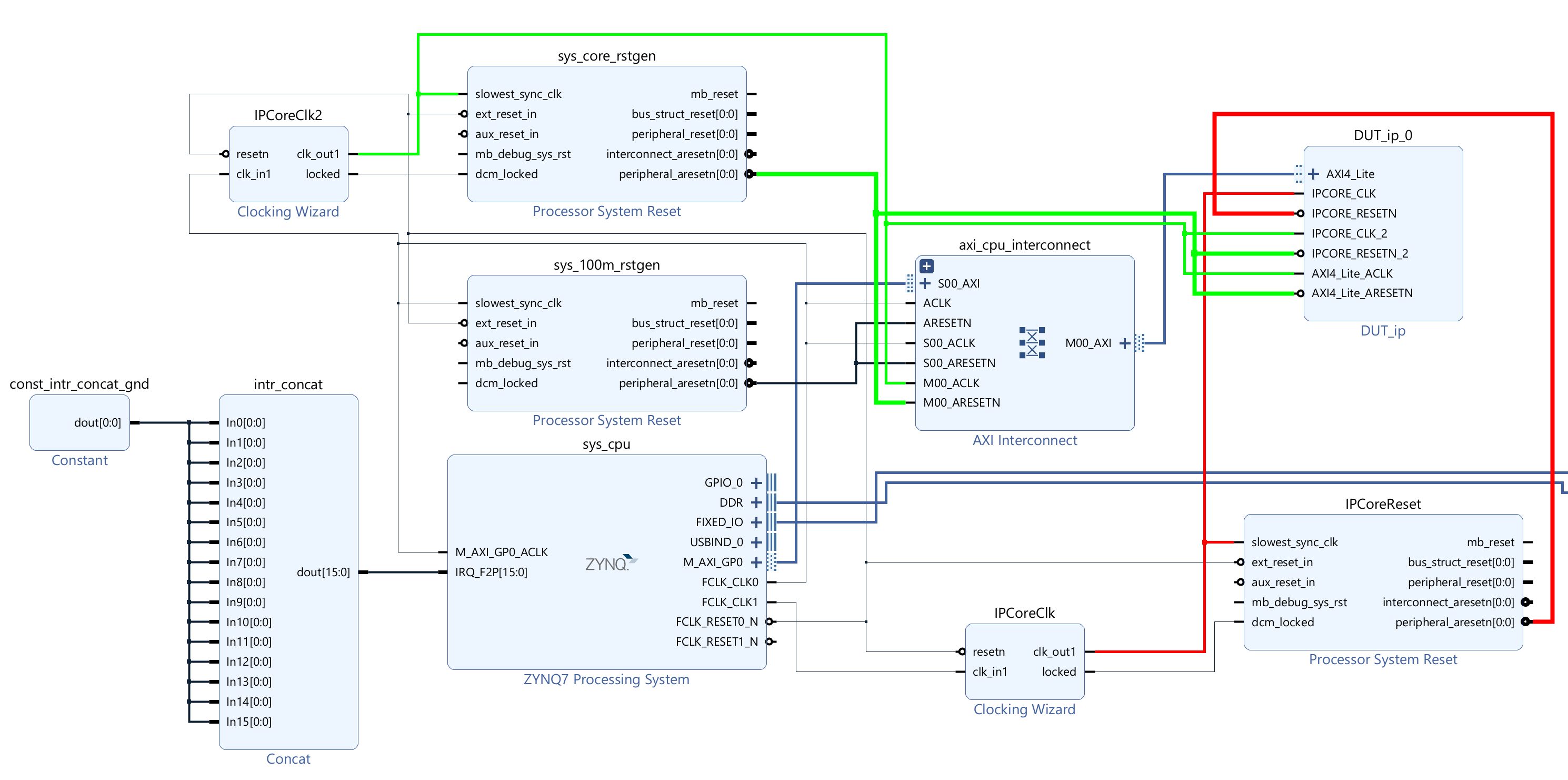
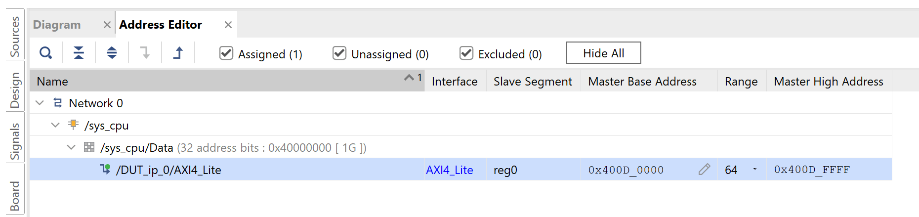
4. Open the Address Editor tab and assign a base address for the DUT. For this example, enter 0x400D0000.
5. Validate the design and click Generate Bitstream.
Interact with FPGA Design from Host Computer
Until you deploy the design to hardware, you cannot simulate metastability and its effects. Use an fpga object to interact with the deployed design, verify the synchronization logic, and compare the counts between the reference, direct, and synchronized data paths.
To use MATLAB to program the ZedBoard, connect to the ZedBoard and interact with the DUT algorithm:
1. Program the FPGA hardware with the generated bitstream and configure the processor with the corresponding device tree. In this example, the device tree necessary to run the system, devicetree_axilite_iio.dtb is available in the firmware image.
hProcessor = xilinxsoc();
programFPGA(hProcessor, "C:\Users\user\CDCExample\hdl_cdc\hdl_cdc.runs\impl_1\system_top_wrapper.bit", "devicetree_axilite_iio.dtb");
2. Create an fpga object for the target device and configure the AXI4-Lite interface to map the DUT ports in the generated HDL IP core. This example code snippet shows the configuration for one of the DUT ports.
hFPGA = fpga(hProcessor);
addRegisterInterface(hFPGA, ...
    "InterfaceID", "AXI4-Lite", ...
    "BaseAddress", 0x400D0000, ...
    "AddressRange", 0x10000, ...
    "WriteDeviceName", "mwipcore0:mmwr0", ...
    "ReadDeviceName", "mwipcore0:mmrd0");
DUTPort_InputRateClkA = hdlcoder.DUTPort("InputRateClkA", ...
	"Direction", "INOUT", ...
	"DataType", numerictype(0,24,0), ...
	"IsComplex", false, ...
	"Dimension", [1 1], ...
	"IOInterface", "AXI4-Lite", ...
	"IOInterfaceMapping", "0x100");
3. Open and run the hdlc_cdc_prototype.m live script. The scrip creates an fpga object, configures AXI4-Lite interfaces to interact wit the DUT ports of the deployed IP core, and then plots the direct, reference, and synchronized counts from the clock A and clock B domains.
open hdlc_cdc_prototype.m
In the Write/Read DUT ports section of the hdlc_cdc_prototype script, this code initializes the rates of the pulse counters to be 4096 and enables them. Then you can read the counts from each counter, the code below does so for 1000 samples.
writePort(hFPGA, "InputRateClkA", 2^12);
writePort(hFPGA, "InputRateClkB", 2^12);
writePort(hFPGA, "SampleRateClkB", 1);
writePort(hFPGA, "SampleRateClkB", 0);
writePort(hFPGA, "EnableVector", [true true]);
for ii=1:N
    vectorCounts = readPort(hFPGA, "VectorOutCounts");
    data_countClkAPulses(ii) = vectorCounts(1);
    data_countClkAPulsesInClkB(ii) = vectorCounts(2);
    data_countSyncClkAPulsesInClkB(ii) = vectorCounts(3);
    data_countClkBPulses(ii) = vectorCounts(4);
    data_countClkBPulsesInClkA(ii) = vectorCounts(5);
    data_countSyncClkBPulsesInClkA(ii) = vectorCounts(6);
end
To visualize the results and verify that the counts when using the CDC synchronizers match the counts in the originating domain for each of the subsystems and the expected behaviors without synchronization, run this code in the hdlc_cdc_prototype.m file:
figure
plot(data_countClkAPulses, :", "LineWidth", 2); hold on
plot(data_countClkAPulsesInClkB, "--", "LineWidth", 2)
plot(data_countSyncClkAPulsesInClkB, "-.", "LineWidth", 2)
legend("ClkA Pulses", "ClkA Pulses in ClkB", "Sync ClkA Pulses in ClkB")

figure
plot(data_countClkBPulses, ":", "LineWidth", 2); hold on
plot(data_countClkBPulsesInClkA, "--", "LineWidth", 2)
plot(data_countSyncClkBPulsesInClkA, "-.", "LineWidth", 2)
legend("ClkB Pulses", "ClkB Pulses in ClkA", "Sync ClkB Pulses in ClkA")
This image shows that when the pulses are synchronized the pulse counts in the clock A and clock B domains are equal.