QPSK Transmitter and Receiver in Simulink
This model shows the implementation of a QPSK transmitter and receiver with Simulink®. The receiver addresses practical issues in wireless communications, such as carrier frequency and phase offset, timing drift and frame synchronization. The receiver demodulates the received symbols and outputs a simple message to the Diagnostic Viewer. For the MATLAB® implementation of the same system, refer to the QPSK Transmitter and Receiver.
Overview
This example model performs all processing at complex baseband to handle a static frequency offset, a timing drift, and Gaussian noise. To cope with the above-mentioned impairments, this example provides a reference design of a practical digital receiver, which includes correlation-based coarse frequency compensation, PLL-based fine frequency compensation, PLL-based symbol timing recovery, frame synchronization, and phase ambiguity resolution. The example showcases a few library blocks in Communications Toolbox™ that implement synchronization algorithms in the receiver processing.
Structure of the Example
The top-level structure of the model is shown in the following figure, which includes the Transmitter subsystem, the channel subsystem, and the Receiver subsystem.

The detailed structures of the Transmitter subsystem and the Receiver subsystem are illustrated in the following figures.


The components are further described in the following sections.
Transmitter
Bit Generation - Generates the bits for each frame
QPSK Modulator - Modulates the bits into QPSK symbols
Raised Cosine Transmit Filter - Uses a rolloff factor of 0.5, and upsamples the QPSK symbols by two
Channel
AWGN Channel with Frequency Offset and Variable Time Delay - Applies the frequency offset, a timing drift, and additive white Gaussian noise to the signal
Receiver
Raised Cosine Receive Filter - Uses a rolloff factor of 0.5
Coarse Frequency Compensation - Estimates an approximate frequency offset of the received signal and corrects it
Symbol Synchronizer - Resamples the input signal according to a recovered timing strobe so that symbol decisions are made at the optimum sampling instants
Carrier Synchronizer - Compensates for the residual frequency offset and the phase offset
Frame Synchronizer - Aligns the frame boundaries at the known frame header
Data Decoding - Resolves the phase ambiguity caused by the Carrier Synchronizer, demodulates the signal, and decodes the text message
Transmitter
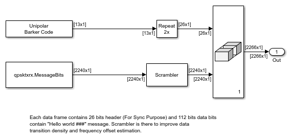
The transmitter includes the Bit Generation subsystem, the QPSK Modulator block, and the Raised Cosine Transmit Filter block. The Bit Generation subsystem uses a MATLAB workspace variable as the payload of a frame, as shown in the figure below. Each frame contains 20 'Hello world ###' messages and a header. The first 26 bits are header bits, a 13-bit Barker code that has been oversampled by two. The Barker code is oversampled by two in order to generate precisely 13 QPSK symbols for later use in the Data Decoding subsystem of the receiver model. The remaining bits are the payload. The payload corresponds to the ASCII representation of 'Hello world ###', where '###' is a repeating sequence of '000', '001', '002', ..., '099'. The payload is scrambled to guarantee a balanced distribution of zeros and ones for the timing recovery operation in the receiver model. The scrambled bits are modulated by the QPSK Modulator (with Gray mapping). The modulated symbols are upsampled by two by the Raised Cosine Transmit Filter with a roll-off factor 0.5. The symbol rate of the transmitter system is 50k symbols per second, and the sample rate after the Raised Cosine Transmit Filter is 100k samples per second.

AWGN Channel with Frequency Offset and Variable Delay
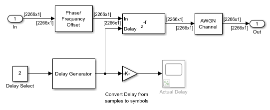
The AWGN Channel with Frequency Offset and Variable Delay subsystem first applies the frequency offset and a preset phase offset to the transmit signal. Then it adds a variable delay with a choice of the following two types of delay to the signal:
Ramp delay - This type of delay is initialized at DelayStart samples, and increases linearly at a rate of DelayStep samples in each frame. When the actual delay reaches one frame, the delay buffer is full, and it maintains a delay of one frame.
Triangle delay - This type of delay linearly changes back and forth between MinDelay samples and MaxDelay samples at a rate of DelayStep samples in each frame
The use of multiple delay characteristics allows you to investigate their effects on receiver performance, particularly on the Symbol Synchronizer block. The delayed signal is processed through an AWGN Channel. The diagram of the AWGN Channel with Frequency Offset and Variable Delay subsystem is as shown in the following.

Receiver
Raised Cosine Receive Filter
The Raised Cosine Receive Filter provides matched filtering for the transmitted waveform with a rolloff factor of 0.5.
AGC
The received signal amplitude affects the accuracy of the carrier and symbol synchronizer. Therefore the signal amplitude should be stabilized to ensure an optimum loop design. The AGC output power is set to a value ensuring that the equivalent gains of the phase and timing error detectors keep constant over time. The AGC is placed before the Raised Cosine Receive Filter so that the signal amplitude can be measured with an oversampling factor of two, thus improving the accuracy of the estimate. You can refer to Chapter 7.2.2 and Chapter 8.4.1 of [ 1 ] for details on how to design the phase detector gain.
Coarse Frequency Compensation
The Coarse Frequency Compensation subsystem corrects the input signal with a rough estimate of the frequency offset. The following diagram shows the subsystem, in which the frequency offset is estimated by averaging the output of the correlation-based algorithm of the Coarse Frequency Compensator block. The compensation is performed by the Phase/Frequency Offset block. There is usually a residual frequency offset even after the coarse frequency compensation, which would cause a slow rotation of the constellation. The Carrier Synchronizer block compensates for this residual frequency.
The accuracy of the Coarse Frequency Compensator decreases with its maximum frequency offset value. Ideally, this value should be set just above the expected frequency offset range. For example, this model introduces a 5 kHz frequency offset and the Coarse Frequency Compensator is configured with a 6 kHz maximum frequency offset.

Symbol Synchronizer
The timing recovery is performed by a Symbol Synchronizer library block, which implements a PLL, described in Chapter 8 of [ 1 ], to correct the timing error in the received signal. The timing error detector is estimated using the Gardner algorithm, which is rotationally invariant. In other words, this algorithm can be used before or after frequency offset compensation. The input to the block is oversampled by two. On average, the block generates one output symbol for every two input samples. However, when the channel timing error (delay) reaches symbol boundaries, there will be one extra or missing symbol in the output frame. In that case, the block implements bit stuffing/skipping thus the output of this block is a variable-size signal.
The Damping factor, Normalized loop bandwidth, and Detector gain parameters of the block are tunable. Their default values are set to 1 (critical damping), 0.01 and 5.4 respectively, so that the PLL quickly locks to the correct timing while introducing little timing jitter.
Carrier Synchronizer
The fine frequency compensation is performed by a Carrier Synchronizer library block, which implements a phase-locked loop (PLL), described in Chapter 7 of [ 1 ], to track the residual frequency offset and the phase offset in the input signal. The PLL uses a Direct Digital Synthesizer (DDS) to generate the compensating phase that offsets the residual frequency and phase offsets. The phase offset estimate from DDS is the integral of the phase error output of a Loop Filter.
The Damping factor and Normalized loop bandwidth parameters of the block are tunable. Their default values are set to 1 (critical damping) and 0.01 respectively, so that the PLL quickly locks to the intended phase while introducing little phase noise.
Frame Synchronizer
The frame synchronization is performed by a MATLAB System block using a FrameSynchronizer System object™. The block uses the known frame header (QPSK-modulated Barker code) to correlate against the received QPSK symbols in order to find the location of the frame header. The block uses this location information to align the frame boundaries. It also transforms the variable-size output of the Symbol Synchronizer block into a fixed-size frame, which is necessary for the downstream processing. The second output of the block is a Boolean scalar indicating if the first output is a valid frame with the desired header and if so, enables the Data Decoding subsystem to run.
Data Decoding
The Data Decoding enabled subsystem performs phase ambiguity resolution, demodulation and text message decoding. The Carrier Synchronizer block may lock to the unmodulated carrier with a phase shift of 0, 90, 180, or 270 degrees, which can cause a phase ambiguity. For details of phase ambiguity and its resolution, please refer to Chapter 7.2.2 and 7.7 in [ 1 ]. The Phase Offset Estimator subsystem determines this phase shift. The Phase Ambiguity Correction & Demodulation subsystem rotates the input signal by the estimated phase offset and demodulates the corrected data. The payload bits are descrambled, and printed out to the Simulink Diagnostic Viewer at the end of the simulation.

Results and Displays
When you run the simulation, it displays bit error rate and numerous graphical results.
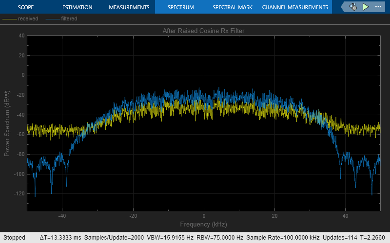
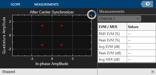
These following scopes illustrate the spectrum of the received signal before and after filtering, as well as the signal constellation after filtering, after timing recovery and after fine frequency compensation.


In the following are the constellation diagrams at the output of the Symbol Synchronizer and Carrier Synchronizer blocks respectively.


Exploring the Example
The example allows you to experiment with multiple system capabilities to examine their effect on bit error rate performance. For example, you can view the effect of changing the frequency offset, delay type and  on the various displays.
This example models a static frequency offset. In practice, the frequency offset might vary over time. This model can still track a time-varying frequency drift via the Coarse Frequency Compensation subsystem. If the actual frequency offset exceeds the maximum frequency offset that can be tracked by the current coarse frequency compensation subsystem, you can increase its tracking range by increasing the oversampling factor. Alternatively, you can change the algorithm from correlation-based to FFT-based, in the Model Parameters block. The FFT-based algorithm performs better than the correlation-based algorithm at low Eb/No.
You can also tune the Normalized loop bandwidth and Damping factor parameters of the Symbol Synchronizer and Carrier Synchronizer blocks, to assess their convergence time and estimation accuracy. In addition, you can assess the pull-in range of the Carrier Synchronizer block. With a large Normalized loop bandwidth and Damping factor, the PLL can acquire over a greater frequency offset range. However a large Normalized loop bandwidth allows more noise, which leads to a large mean squared error in the phase estimation. "Underdamped systems (with Damping Factor less than one) have a fast settling time, but exhibit overshoot and oscillation; overdamped systems (with Damping Factor greater than one) have a slow settling time but no oscillations." [ 1 ]. For more detail on the design of these PLL parameters, you can refer to Appendix C in [ 1 ].
References
1. Michael Rice, "Digital Communications - A Discrete-Time Approach", Prentice Hall, April 2008.